

Method of fabrication of a finfet element
A fin field effect and manufacturing method technology, which is applied in semiconductor/solid-state device manufacturing, semiconductor devices, electrical components, etc., can solve the problems of low ion energy and inability to meet the performance of fin field effect transistors, and meet the performance requirements Effect
- Summary
- Abstract
- Description
- Claims
- Application Information
AI Technical Summary
Problems solved by technology
Method used
Image

Examples
Embodiment Construction
[0051]The manner in which the various embodiments can be made and used are described in detail below. However, it is worth noting that the various applicable inventive concepts provided by the present invention can be implemented according to various changes in the specific content, and the specific embodiments discussed here are only used to show the specific use and manufacture of the present invention method without limiting the scope of the present invention.
[0052] The manufacturing process of the preferred embodiment of the present invention is illustrated below through various drawings and examples. In addition, the same symbols represent the same or similar elements in various different embodiments and drawings of the present invention.
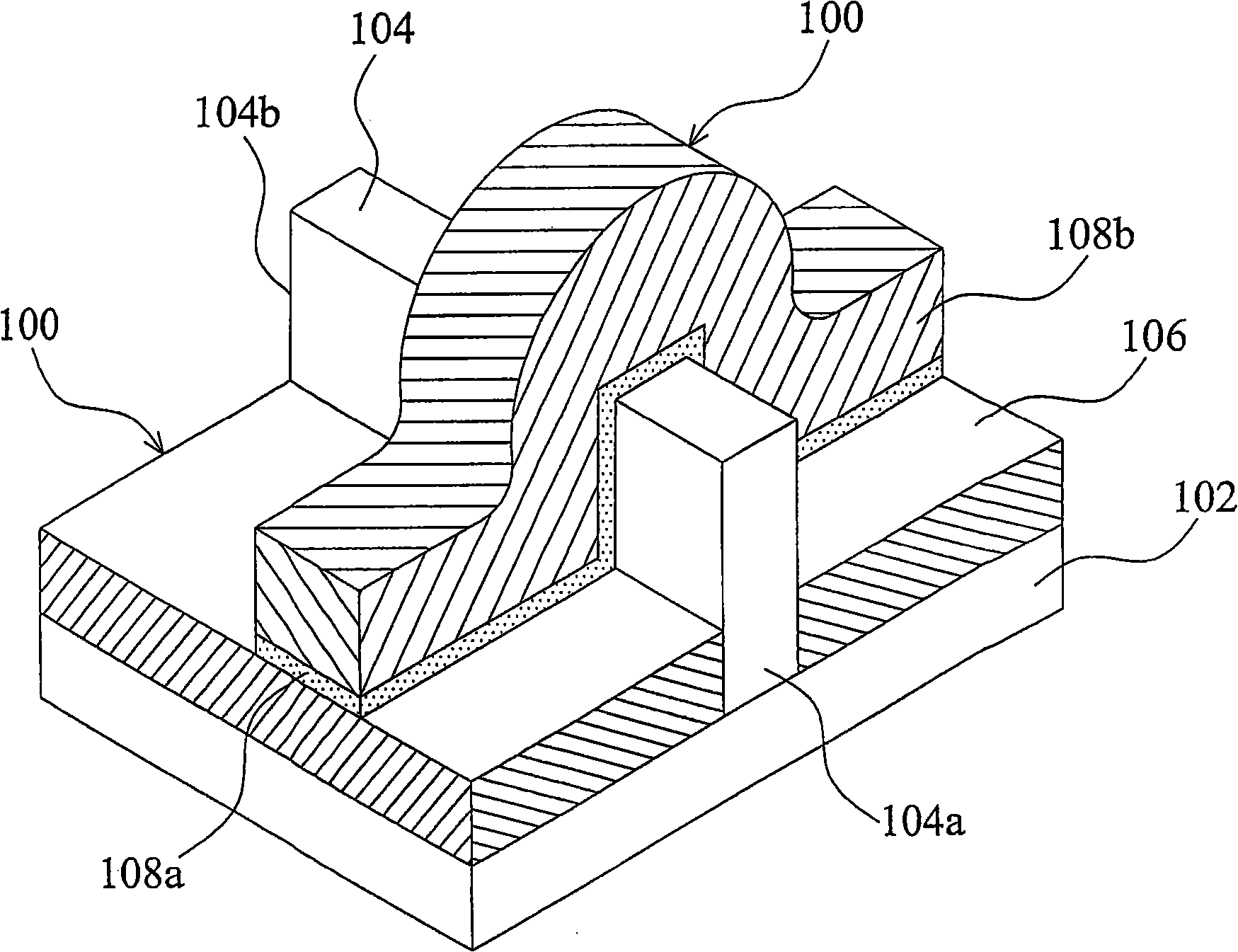
[0053] figure 1 An embodiment of a FinFET device 100 is shown. The FinFET device 100 includes a substrate 102 , an insulating layer 106 , a fin 104 , and a gate structure 108 . In an embodiment, substrate 102 includes a silicon ...
PUM
 Abstract
Description
Claims
Application Information