

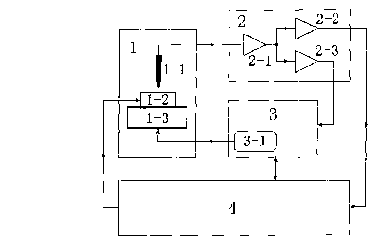
Scanning-tunnelling microscope for vibrating example and measurement method thereof
A technology of scanning tunneling and measurement methods, applied in scanning probe microscopy, measurement devices, scanning probe technology, etc., can solve the problems of not being able to identify what kind of atoms or molecules are being observed, and low resolution.
- Summary
- Abstract
- Description
- Claims
- Application Information
AI Technical Summary
Problems solved by technology
Method used
Image

Examples
Embodiment 1
[0034] Example 1: Realize atomic discrimination
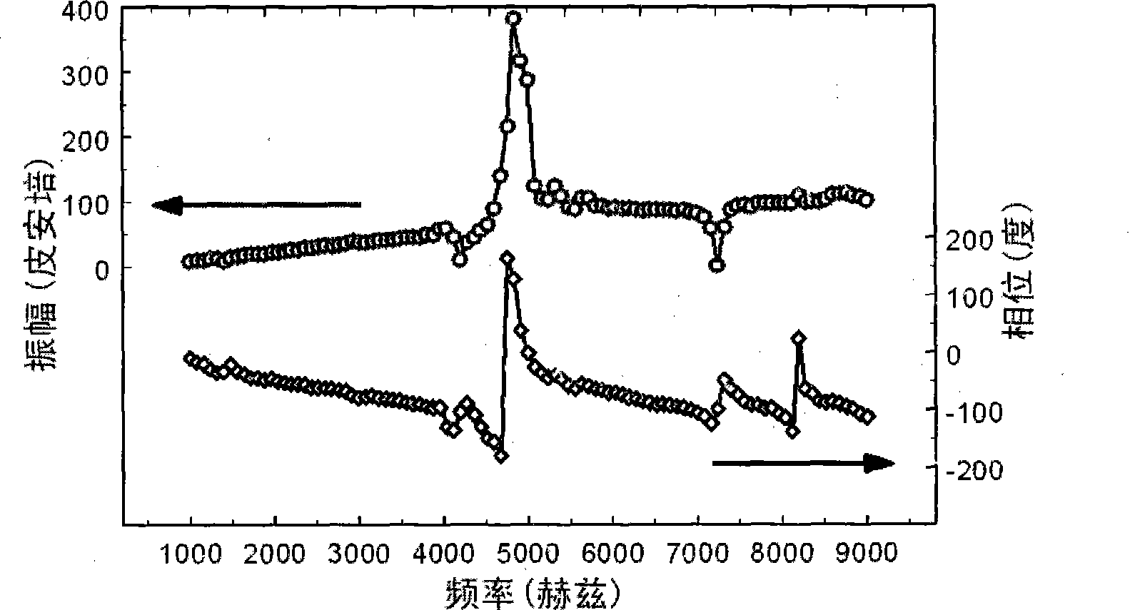
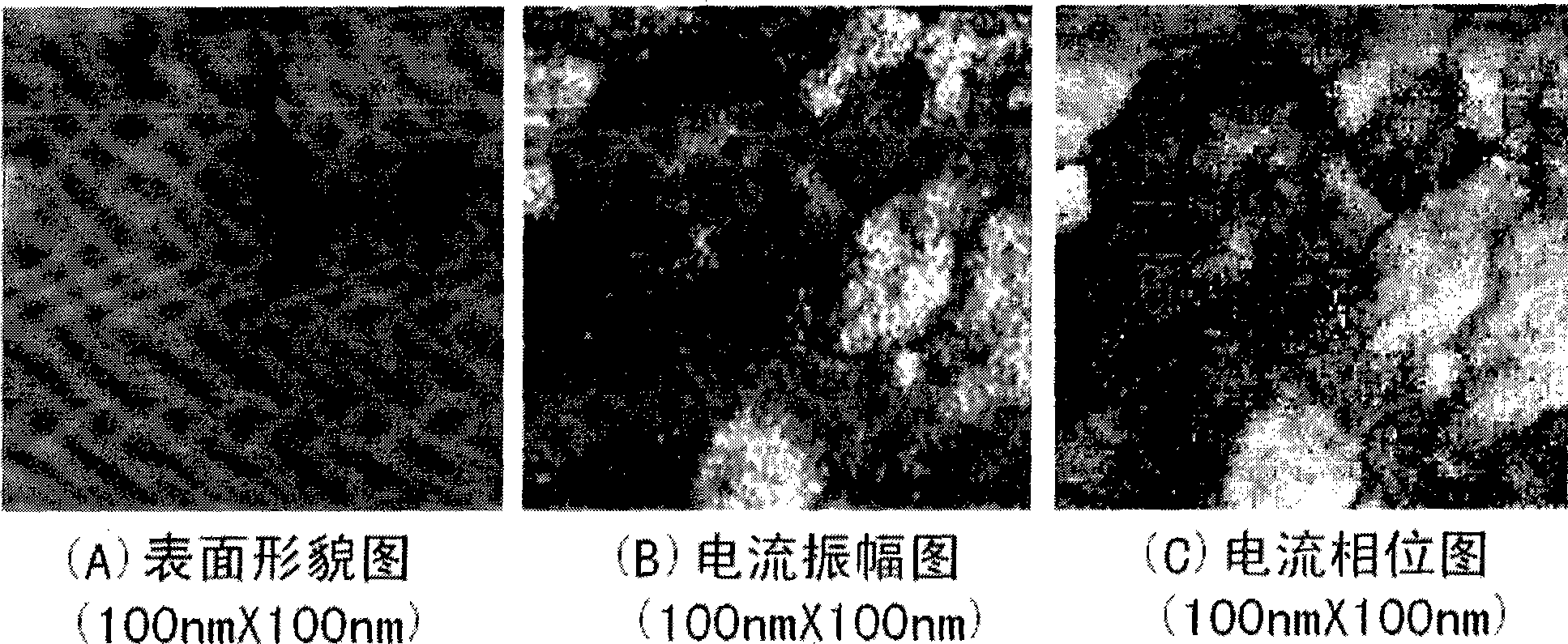
[0035] attached image 3 The STM topography diagram, the amplitude diagram and the phase diagram of the alternating tunneling current signal measured simultaneously by the invention are given. The measurement conditions are: tunnel current 0.8nA, sample bias voltage 0.1V; AC excitation signal peak-to-peak value 1.0V, AC excitation signal frequency 5kHz.
[0036] Within this scanning range, micro-regions composed of platinum and gold are likely to exist on the surface of the sample at the same time. From the topography, many crystal grains can be seen, but the region composed of these two elements cannot be distinguished. But on the current amplitude diagram and the phase diagram, there are two distinct regions, and the region with smaller current amplitude corresponds to the region with smaller phase. The mechanical properties of platinum and gold are similar, and the intensity of the effective excitation signal in the micro-r...
Embodiment 2
[0037] Embodiment 2: Resolving multi-phase alloy materials:
[0038] attached Figure 4 The STM surface topography diagram, the amplitude diagram and the phase diagram of the alternating tunnel current signal measured by the present invention are given. Before the test, after grinding and polishing, a layer of platinum atoms was sputtered on the surface to enhance its surface conductivity. The measurement conditions are: tunnel current 0.8nA, sample bias voltage 0.1V; AC excitation signal peak-to-peak value 2.0V, AC excitation signal frequency 15kHz.
[0039] Sn-Pb alloy is a typical two-phase coexistence alloy material. From the topography, there are many grains, but the regions of these two different phases cannot be distinguished. But on the current amplitude map and phase map, there are two distinct areas, the area with smaller current amplitude corresponds to the area with smaller phase; in the dark area in the lower left corner, there is also a small bright area . I...
PUM
 Abstract
Description
Claims
Application Information