Vertical structure semiconductor devices

A semiconductor and device technology, applied in the field of GaN-based vertical structure semiconductor devices

Inactive Publication Date: 2009-02-11
VERTICLE
View PDF0 Cites 16 Cited by
  • Summary
  • Abstract
  • Description
  • Claims
  • Application Information

AI Technical Summary

Problems solved by technology

Perforated metal wafer carriers are also used for wafer bonding for easy handling and debonding

Method used


Image

  • Vertical structure semiconductor devices
  • Vertical structure semiconductor devices
  • Vertical structure semiconductor devices

Examples


Embodiment Construction

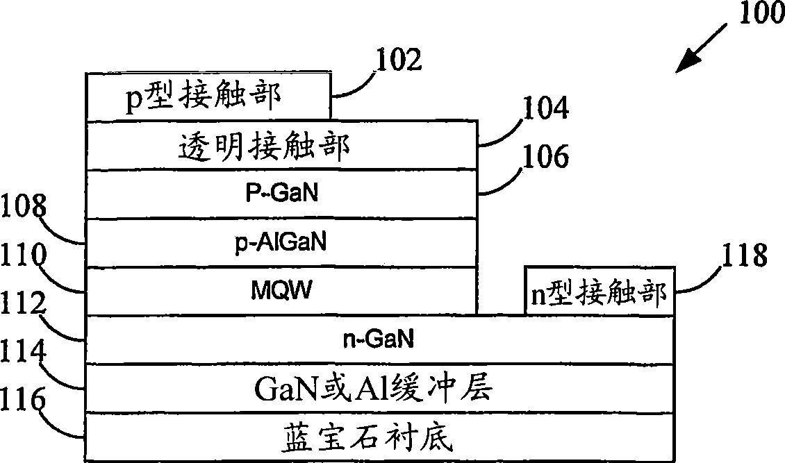
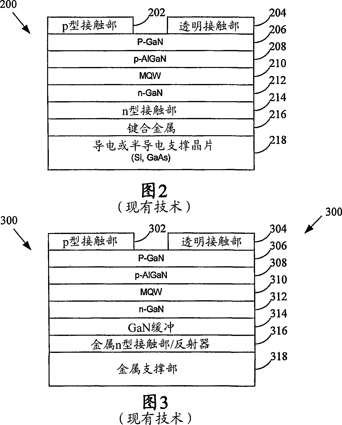
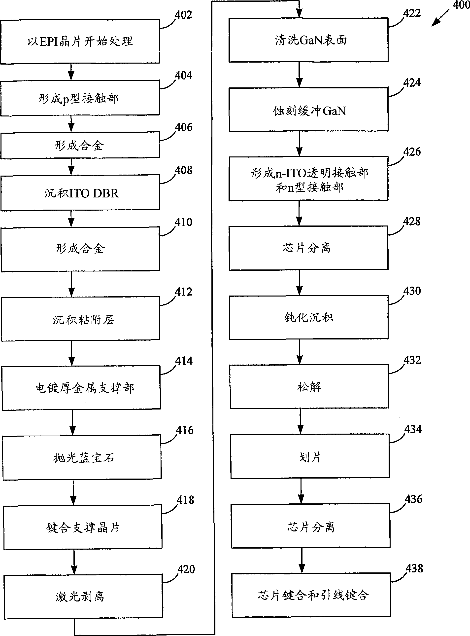
[0033] The invention is described with reference to specific device structures and embodiments. Those skilled in the art should understand that the description is illustrative and provides the best mode for carrying out the invention. The present invention includes a number of formation and deposition steps for fabricating a semiconductor device according to the present invention. This disclosure relates to depositing materials on or over other materials, which are illustrated and described as representing any box with reference, as explained and understood by a person skilled in the art in conjunction with the description, and this disclosure is intended to describe and overlay on top of other materials Techniques for depositing material over, over, or under. For example, some parts of this disclosure describe semiconductor layers constructed from above and other parts describe semiconductor layers constructed from below, and in both cases, as illustrated and shown, the depo...


PUM


Abstract

The invention provides a reliable way to fabricate a new vertical structure compound semiconductor device with improved light output and a laser lift-off processes for mass production of GaN-based compound semiconductor devices. A theme of the invention is employing direct metal support substrate deposition prior to the LLO by an electro-plating method to form an n-side top vertical structure. In addition, an ITO DBR layer is employed right next to a p-contact layer to enhance the light output by higher reflectivity. A perforated metal wafer carrier is also used for wafer bonding for easy handling and de-bonding. A new fabrication process is more reliable compared to the conventional LLO-based vertical device fabrication. Light output of the new vertical device having n-side up structure is increased 2 or 3 times higher than that of the lateral device fabricated with same GaN / InGaN epitaxial films.

Description

technical field [0001] The present invention relates to the fabrication of a GaN-based vertical structure semiconductor device with top and bottom contact structures and a method for fabricating the vertical structure device. Background technique [0002] FIG. 1 shows a conventional gallium nitride (GaN)-based (GaN-based) semiconductor device 100 fabricated on an insulating sapphire substrate 114 . The device can be used in applications such as Light Emitting Diodes (LEDs), Laser Diodes (LDs), Heterojunction Bipolar Transistors (HBTs), and High Electron Mobility Transistors (HEMTs). In a conventional process, the device is formed on a sapphire substrate, and two electrical contacts are formed on top of the device. A p-contact 102 is formed on top, and a mesa etch is used to remove material to form an n-metal contact 118 . The result is known as a lateral structure device and tends to exhibit several problems including poor resistance to electrostatic discharge (ESD) and he...

Claims


Application Information

Patent Timeline
Patent Type & Authority Applications(China)
IPC IPC(8): H01L29/00H01L21/00H01L21/268H01L29/22H01L33/00H01S5/02H01S5/024H01S5/042H01S5/183H01S5/343
CPCH01L33/32H01L21/268H01L33/0079H01L33/46B82Y20/00H01L2224/85181H01L2224/48463H01L2224/73265H01L2224/45144H01L33/0093H01L2924/00H01L33/12H01L33/36
Inventor 刘明哲
Owner VERTICLE
Why Eureka
Try Eureka