Unlock instant, AI-driven research and patent intelligence for your innovation.

Semiconductor device, wafer coarse alignment mark and coarse alignment method

A semiconductor, rough alignment technology, applied in the direction of semiconductor devices, semiconductor/solid-state device manufacturing, semiconductor/solid-state device components, etc. Mark precision alignment failure and other problems to achieve the effect of improving the success rate

Active Publication Date: 2010-06-09
SEMICON MFG INT (SHANGHAI) CORP
View PDF3 Cites 0 Cited by
  • Summary
  • Abstract
  • Description
  • Claims
  • Application Information

AI Technical Summary

Problems solved by technology

[0010] The present invention provides a semiconductor device, a rough alignment mark of a wafer and a rough alignment method, which solves the problem that the fine alignment mark cannot be found in the fine alignment of lithography in the prior art and the fine alignment fails, so that the lithography cannot continue question

Method used


Image

  • Semiconductor device, wafer coarse alignment mark and coarse alignment method
  • Semiconductor device, wafer coarse alignment mark and coarse alignment method
  • Semiconductor device, wafer coarse alignment mark and coarse alignment method

Examples


Embodiment Construction

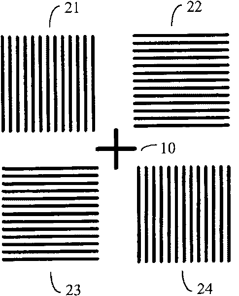
[0033] The structure of the rough alignment mark of the semiconductor device, the rough alignment mark of the wafer and the rough alignment method of the present invention is similar to that of the alignment mark used for the calibration of the lithography device. The alignment marks are exposed, developed and etched at the same time in the previous process, so they are well coupled with the fine alignment marks in the lithography device. Therefore, the rough wafer alignment marks of the above scheme can improve the precision alignment of the lithography device. The success rate of finding fine alignment marks during the process.

[0034] The semiconductor device, the rough alignment mark of the wafer and the rough alignment method of the present invention are described in detail through the preferred embodiments, so that the rough alignment mark of the wafer and the rough alignment method of the present invention are more clear.

[0035] refer to figure 1 As shown, the rough...


PUM


Abstract

The invention discloses a wafer coarse alignment mark, comprising: a first structure and a second structure distributed around the first structure; the first structure is in a shape of cross, the second structure comprises four groups of gratings in which two adjacent groups of gratings are perpendicular to one another. The invention also discloses a semiconductor device and a coarse alignment method. The inventive semiconductor device, wafer coarse alignment mark and coarse alignment method strengthen success ratio of precise alignment on account of addressing the problem of failing to precisely align the wafers after the coarse alignment in the prior art.

Description

technical field [0001] The invention relates to a photolithography process, in particular to a semiconductor device, a wafer rough alignment mark and a rough alignment method in the photolithography process. Background technique [0002] With the development of semiconductor technology, the area of ​​semiconductor chips is getting smaller and smaller, and the line width in the chip is also shrinking. Therefore, the test of semiconductor process capability is also increasing, and the control of process accuracy and process variation has also become more and more important. more important. In the process of manufacturing semiconductor chips, the most important process is lithography, which is a process of transferring the mask pattern to the wafer through a series of steps such as alignment, exposure, and etching. Therefore, lithography The quality of the process will directly affect the performance of the final chip. [0003] At present, there are mainly two kinds of device...

Claims


Application Information

Patent Timeline
Patent Type & Authority Patents(China)
IPC IPC(8): H01L23/544H01L21/68
Inventor 杨晓松
Owner SEMICON MFG INT (SHANGHAI) CORP