Packaging structure and method for high power white light LED
A technology of light-emitting diodes and packaging structures, applied in electrical components, electrical solid-state devices, circuits, etc., can solve the problems of not getting rid of the traditional module packaging method, and achieve the effect of improving the light-emitting effect, reducing the probability of total reflection, and improving the light-emitting effect.
- Summary
- Abstract
- Description
- Claims
- Application Information
AI Technical Summary
Problems solved by technology
Method used
Image
Examples
Embodiment 1
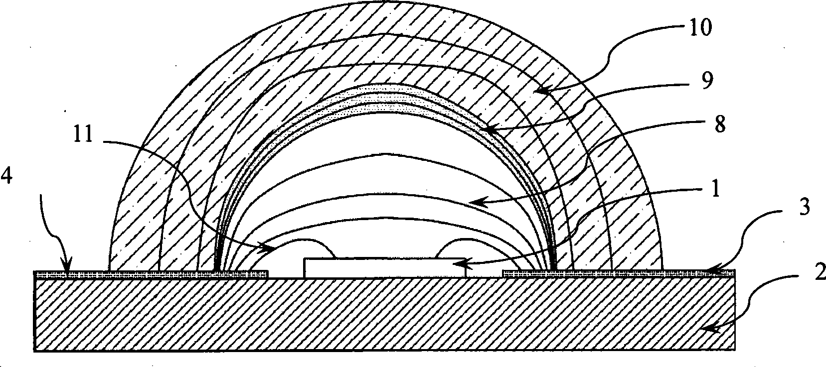
[0033] see figure 1 The LED chip 1 is welded in the chip bonding area of the substrate 2, and the positive and negative electrodes of the chip 1 are connected to the first electrode 3 and the second electrode 4 of the circuit layer of the substrate 2 through the gold wire 11. The LED chip 1 is covered by multiple layers of inner sealing colloids 8 of different shapes, the outer surface of the inner sealing colloid 8 is covered by multiple layers of phosphor adhesive layers 9 of different shapes, and the outer surface of the phosphor adhesive layer 9 is covered by multiple layers of different shapes. The outer envelope lens 10 covers.
[0034] The type of the LED chip 1 in this embodiment is not limited, and the type of the substrate 2 and the positions of the first electrode 3 and the second electrode 4 on the circuit layer of the substrate 2 can be adjusted according to the type of the chip 1 .
[0035] In this embodiment, the number of layers of inner sealing colloid 8, f...
Embodiment 2
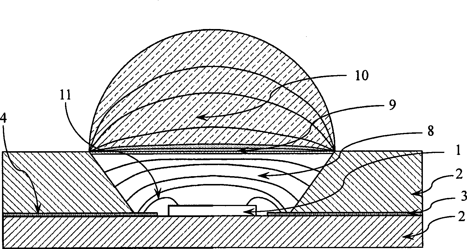
[0050] Embodiment 2 is the same as Embodiment 1, except that the substrate 2 of Embodiment 2 is a double-layer substrate, see figure 2 , there is a recessed reflective cup on the substrate 2, and the chip 1 is located at the bottom of the reflective cup. In addition, the forming method of each layer of colloid of the inner sealing colloid 8 is the injection mode, see Figure 11 . The colloid of each layer of the fluorescent powder adhesive layer 9 is formed by injection, and each layer of the outer sealing lens 9 is formed by molding or potting.
Embodiment 3
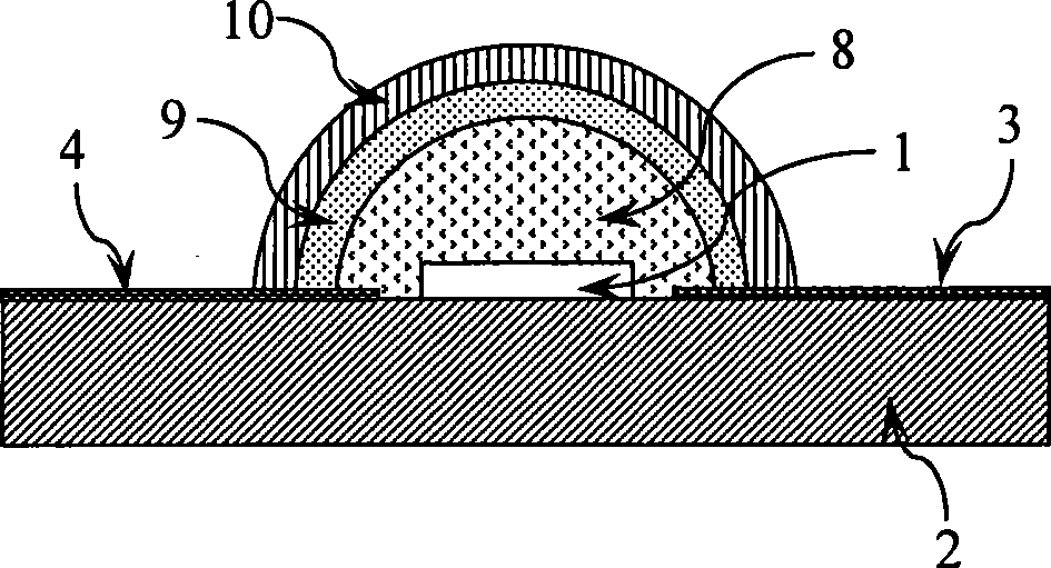
[0052] Embodiment 3 is the same as Embodiment 1, except that the inner sealing colloidal layer 8, the fluorescent powder adhesive layer 9, and the outer sealing lens 10 of the third embodiment are all single layers, and the inner sealing colloidal layer 8 is formed by potting, and the fluorescent The powder layer 9 is formed by potting, and the outer sealing lens 10 is formed by injection or molding. see image 3 .
PUM
 Abstract
Description
Claims
Application Information


