Stress buffering package for a semiconductor component

A stress buffer, semiconductor technology, applied in semiconductor devices, semiconductor/solid-state device components, electric solid-state devices, etc., can solve problems such as the influence of electronic circuits, and achieve the effect of reducing the surface area

Active Publication Date: 2011-04-13
NXP BV
View PDF4 Cites 0 Cited by
  • Summary
  • Abstract
  • Description
  • Claims
  • Application Information

AI Technical Summary

Problems solved by technology

In addition, the materials contained in the conductive layer 18 also have some problems in the manufacture of semiconductors, especially wafers.
The use of materials such as copper or gold can cause electronic circuits in silicon to be affected

Method used


Image

  • Stress buffering package for a semiconductor component
  • Stress buffering package for a semiconductor component
  • Stress buffering package for a semiconductor component

Examples


Embodiment Construction

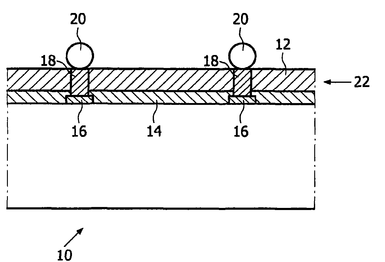
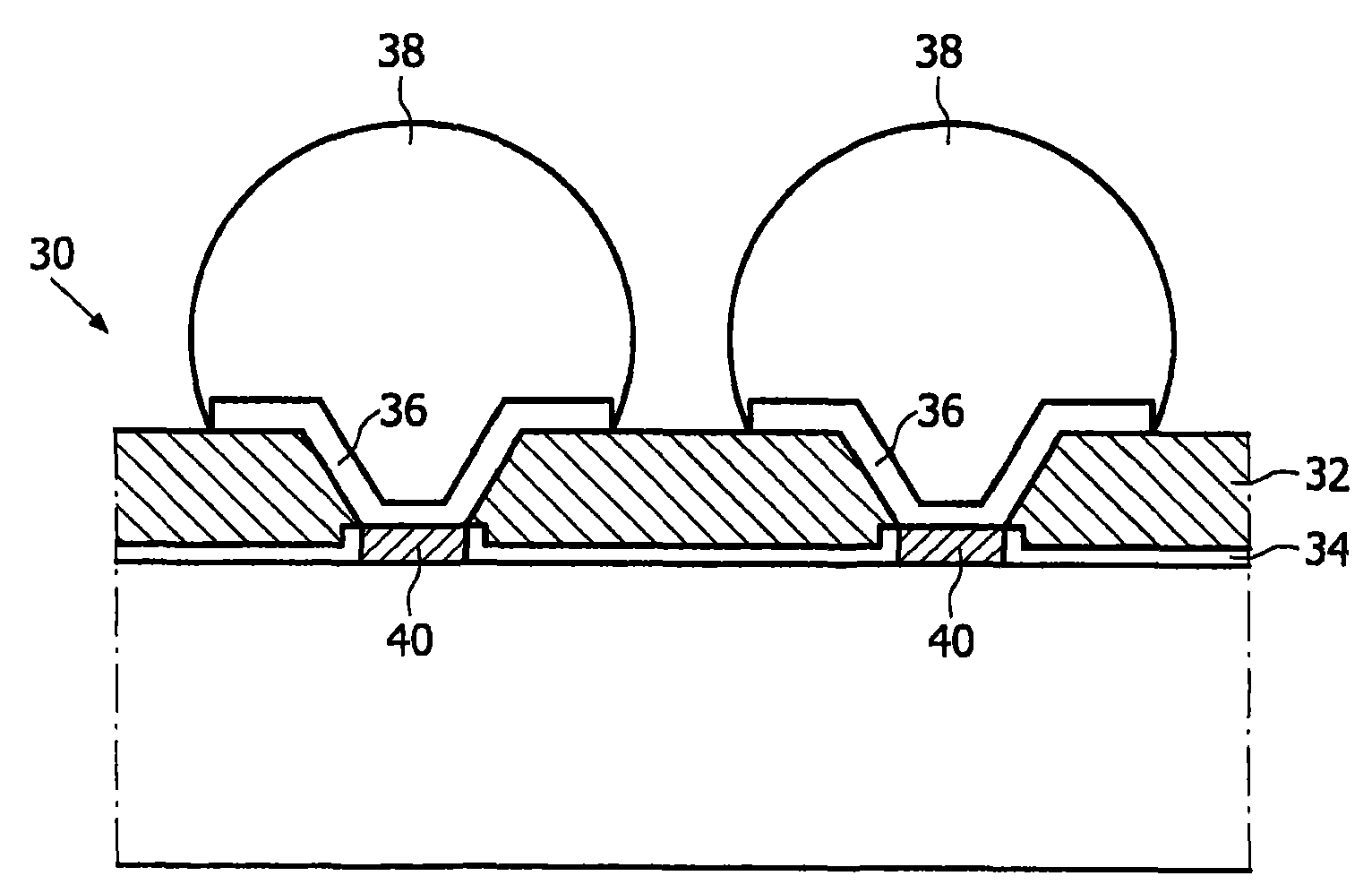
[0037] figure 1 with 2 An encapsulation according to the prior art is shown, discussed above.

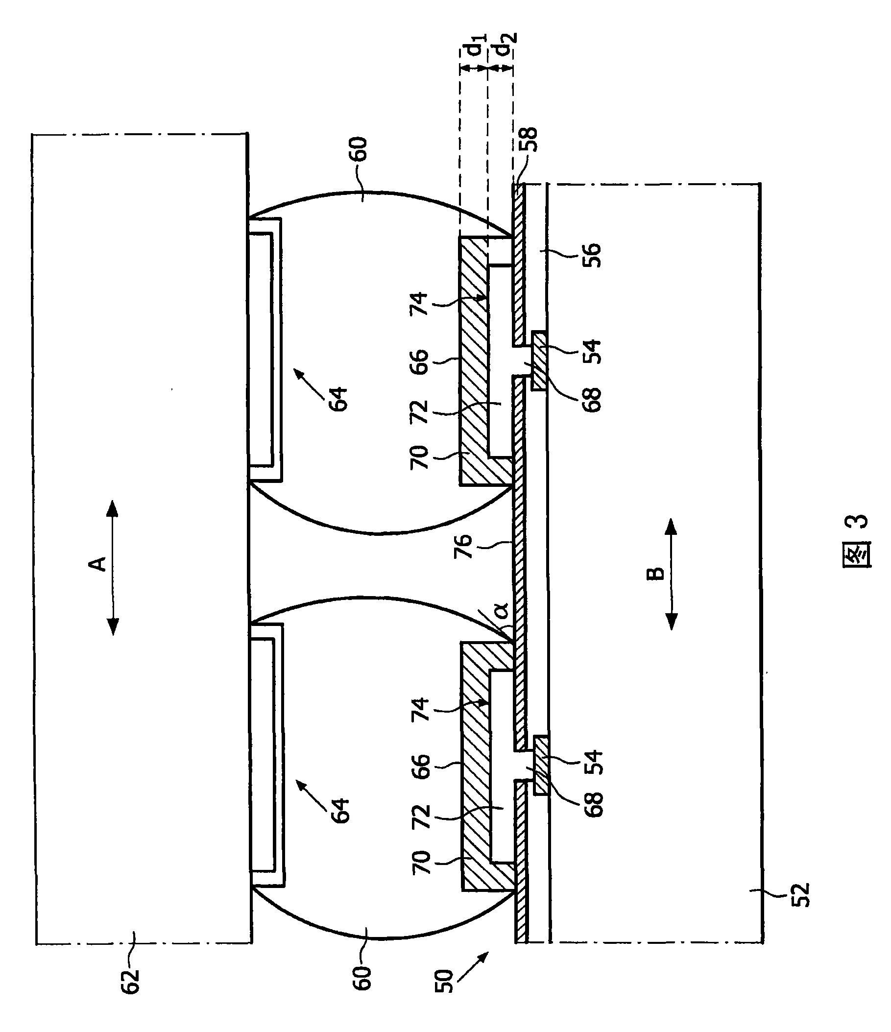
[0038] FIG. 3 shows a stress buffer package 50 for a semiconductor 52 including a plurality of I / O pads 54 on its upper surface. The semiconductor also includes a passivation layer 56 that protects the active regions of the semiconductor and exposes the I / O pads. Preferably, the passivation layer comprises silicon oxide. An additional passivation layer 58 of silicon nitride is usually applied on the passivation layer 56 .

[0039] The function of the solder balls 60 is to electrically connect the semiconductor 52 or another electrical component to the end of the board 62 where the electrodes 64 are disposed. The I / O pads and solder balls are electrically connected through the underball metallization 70 and the stress buffer element 74 . The outer surface of the under-ball metallization 70 forms a so-called bond pad 66, which makes it possible to place a solder ball.

[0040] E...


PUM

PropertyMeasurementUnit
thicknessaaaaaaaaaa
thicknessaaaaaaaaaa
elastic modulusaaaaaaaaaa

Abstract

The present invention relates to a stress buffering package for a semiconductor component, wherein a stress buffering means comprises individual stress buffering elements that do not influence the stress buffering effect from each other. Furthermore the invention relates to a method for manufacturing a stress buffering package for a semiconductor component.

Description

technical field [0001] The invention relates to a stress-buffering package of a semiconductor component according to the preamble of claim 1 . The concern here is the so-called chip-scale packaging. Electronic components, which may include, for example, diodes, transistors, MEMS (micro-electromechanical elements) or capacitors, are mounted on a substrate such as a printed circuit board by means of solder balls without additional carriers. Chip-scale packaging is especially used for so-called power transistors and ESD (electrostatic discharge) diodes, often combined with passive filters including resistors, capacitors and / or coils. Chip scale packaging is also used in particular in FM (Frequency Modulation) radios. This is a semiconductor with amplifiers and tuners and any other circuitry that may be required to fully perform the radio functions of a mobile phone. The size of the package is an essential factor in this case, partly because of the small space available in mobi...

Claims


Application Information

Patent Timeline
Patent Type & Authority Patents(China)
IPC IPC(8): H01L23/485
CPCH01L2924/014H01L2924/01005H01L2224/13099H01L2924/0105H01L2924/01015H01L2924/01006H01L2924/01019H01L2924/01078H01L2924/01012H01L24/10H01L2924/01047H01L2924/01013H01L2924/01029H01L2924/05042H01L2924/01082H01L2924/19043H01L2924/01004H01L2224/16H01L2924/01023H01L24/02H01L2924/01046H01L2924/01079H01L2924/19041H01L2924/01014H01L2224/0401H01L2924/01033H05K3/3436H01L2924/01028H05K1/0271H01L24/13H01L2924/1461H01L2924/351H01L2224/13H01L2224/16238H01L2224/16013H01L2224/05562H01L2224/05027H01L2224/05019H01L24/05H01L24/16H01L2224/02125H01L2924/00
Inventor 亨德里克·P·胡切斯坦巴赫
Owner NXP BV
Why Eureka
Try Eureka