
Fine mask and method of forming mask pattern using the same

A mask pattern and mask technology, which is applied in the photoengraving process of the pattern surface, the original for opto-mechanical processing, optics, etc. Resolution, the effect of improving accuracy

Inactive Publication Date: 2009-02-25
DONGBU HITEK CO LTD
View PDF1 Cites 3 Cited by
  • Summary
  • Abstract
  • Description
  • Claims
  • Application Information

AI Technical Summary

Problems solved by technology

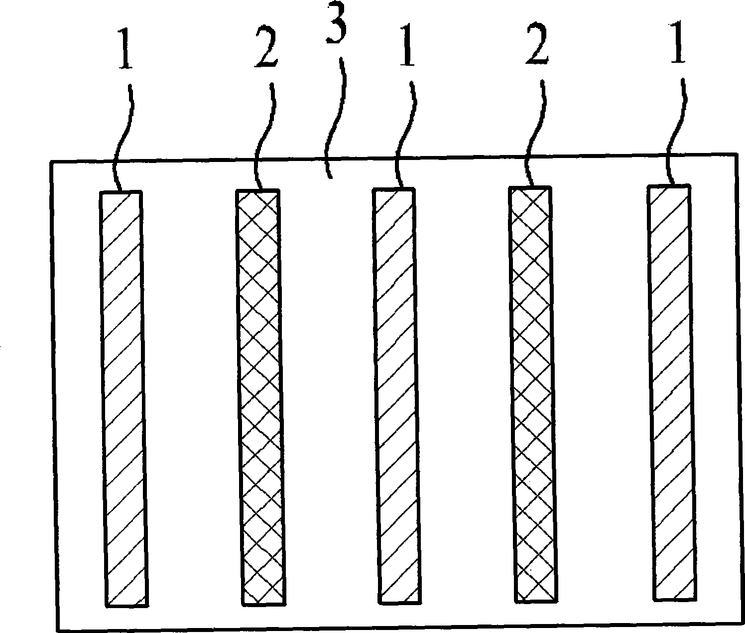
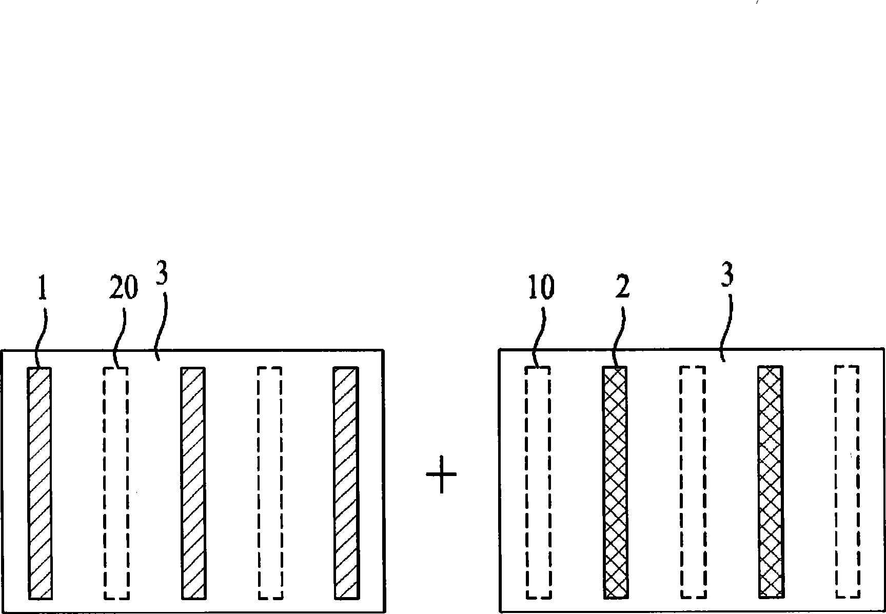
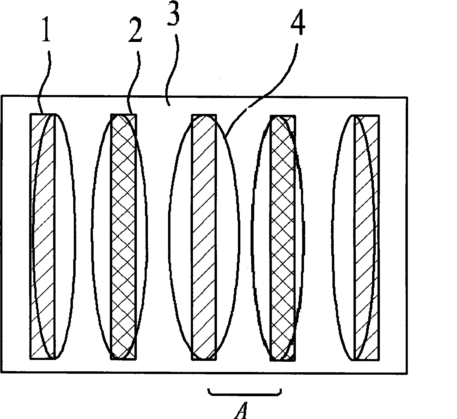
However, when based on related technologies, such as Figure 1B The two masks shown are aligned and exposed in the exposure setup, as Figure 1C As shown in the exposure profile image 4, when the patterns formed by exposure are close to each other, as Figure 1C The linewidth resolution shown in part A is severely degraded

Method used


Image

  • Fine mask and method of forming mask pattern using the same
  • Fine mask and method of forming mask pattern using the same
  • Fine mask and method of forming mask pattern using the same

Examples


Embodiment Construction

[0024] figure 2 is a schematic diagram of a mask of a double exposure mask according to an embodiment of the present invention. image 3 is a schematic diagram of another mask of a double exposure mask according to an embodiment of the present invention. Figure 4 shows when figure 2 mask as shown and as image 3 The photoresist pattern image obtained when the mask is aligned and exposed is shown.

[0025] figure 2 and image 3 shows two masks, and Figure 4 Two masks are shown optically overlapping each other. In the example, when as figure 2 mask as shown and as image 3 When the masks shown overlap each other, the masks are arranged so that the main patterns of the respective masks do not overlap each other. That is, when figure 2 and image 3 When the two masks in the mask overlap with each other, the positions where the main patterns of the respective masks are located do not overlap with each other.

[0026] In the following description, the figure 2 m...


PUM

PropertyMeasurementUnit
transmittivityaaaaaaaaaa

Abstract

In a semiconductor technology, a fine mask for a semiconductor and a method of forming a mask pattern using the same are disclosed. In order to improve accuracy of line width resolution and optical resolution in forming a pattern of a semiconductor wafer, the fine mask includes a first mask, including a first mask original plate, a first light-blocking pad pattern formed on the first mask original plate, a first main pattern including a plurality of first light-transmitting regions formed on the first light-blocking pad pattern, and a first sub-pattern including a plurality of phase shift regions between the first light-transmitting regions and at an outermost portion of the first mask original plate. A second mask includes a second mask original plate, a second light-blocking pad pattern formed on the second mask original plate, a second main pattern including a plurality of second light-transmitting regions formed on the second light-blocking pad pattern, and a second sub-pattern including a plurality of phase shift regions between the second light-transmitting regions.

Description

[0001] This application claims priority under US Law Section 119-35 of Korean Patent Application No. 10-2007-0083536 (filing date Aug. 20, 2007), the entire contents of which are incorporated herein by reference. technical field [0002] The invention relates to semiconductor technology, in particular to a fine mask for semiconductors and a method for forming mask patterns using the fine mask. Background technique [0003] Now, as mask designs become more detailed, photolithography can be used to properly adjust the amount of light transmitted through the mask. Likewise, new photoresists, scanners with high numerical aperture lenses, and improved masking techniques were developed to overcome various technical limitations in fabricating devices. In particular, Optical Proximity Correction (OPC) is very beneficial for overcoming technical limitations in optical exposure devices. Therefore, the optical distortion phenomenon can be effectively overcome by optical proximity corr...

Claims


Application Information

Patent Timeline
Patent Type & Authority Applications(China)
IPC IPC(8): G03F1/14
CPCG03F1/36G03F1/144G03F1/26G03F1/70H01L21/0274
Inventor 李峻硕
Owner DONGBU HITEK CO LTD
Learn More