Semiconductor foreign substrate and growing method thereof

A technology of heterogeneous substrates and growth methods, applied in semiconductor devices, semiconductor/solid-state device manufacturing, electrical components, etc., can solve problems such as sample bending, cracks, lack of stress release layers, etc., to improve crystal quality and reduce stress. Effect

Inactive Publication Date: 2009-03-04
SUZHOU NANOWIN SCI & TECH
View PDF0 Cites 38 Cited by
  • Summary
  • Abstract
  • Description
  • Claims
  • Application Information

AI Technical Summary

Problems solved by technology

[0005] In the prior art, after the growth of these materials, there is a lack of a stress release layer, resulting in huge stress in the semiconductor heterogeneous substrate after growth, resulting in the sample being in a bent state, or even cracks, affecting the subsequent device process and performance. It has a great negative impact, and in severe cases, it can cause the substrate to be unusable in the subsequent process and become a waste product

Method used


Image

  • Semiconductor foreign substrate and growing method thereof
  • Semiconductor foreign substrate and growing method thereof
  • Semiconductor foreign substrate and growing method thereof

Examples


Embodiment Construction

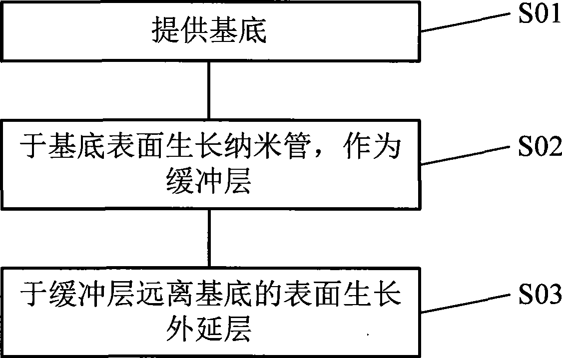
[0020] The specific implementation of the semiconductor heterogeneous substrate and its growth method provided by the present invention will be given below with reference to the accompanying drawings.

[0021] Firstly, a specific implementation manner of the semiconductor heterogeneous substrate described in the present invention will be given with reference to the accompanying drawings.

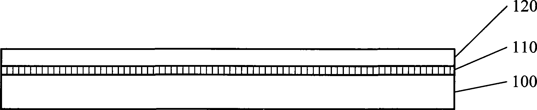
[0022] attached figure 1 It is a schematic diagram of the semiconductor heterogeneous substrate structure described in this specific embodiment, including a base layer 100, an epitaxial layer 120, and a buffer layer 110 sandwiched between the base layer 110 and the epitaxial layer 120, and the buffer layer 110 is a nanotube material .

[0023] The base layer 100 is a sapphire substrate, the epitaxial layer is a GaN layer, and the nanotubes are carbon nanotubes or group III nitride nanotubes.

[0024] The nanotubes may be single-walled or multi-walled nanotubes. The orientation of the nano...


PUM


Abstract

The invention provides a foreign substrate of the semiconductor, comprising a substrate layer, an epitaxial layer and a buffer layer with nanotube materials between the substrate layer and the epitaxial layer. The invention also provides a growth method for the foreign substrate of the semiconductor. The invention has the advantages that: by adopting the buffer layer with nanotube materials and making use of the properties of the flexible linkage of the nanotube, the lattice mismatch and thermal mismatch between the epitaxial layer and the substrate layer are eliminated, so as to reduce the stress in the epitaxial layer; as to the provided growth method, during the growth process of the epitaxial layer on the surface of the nanotube, the nanotube as a nucleation center during the epitaxial process of the epitaxial materials is used for forming high-quality crystal nucleus at the initial epitaxial stage, thus being beneficial to improving the crystal quality of the epitaxial layer.

Description

【Technical field】 [0001] The invention relates to a semiconductor material and a growth method of the semiconductor material, in particular to a semiconductor heterogeneous substrate and a growth method thereof. 【Background technique】 [0002] With the continuous development and progress of the information society, semiconductor materials are more and more widely used in people's lives. Silicon materials are mainly used in the field of integrated circuits, compound semiconductor materials are mainly used in semiconductor lighting and display fields, and various semiconductor materials are also used in large quantities in many other fields. [0003] Most of the widely used semiconductor materials are crystalline materials, which are difficult to exist in nature. Therefore, it is necessary to study the methods of growing crystalline semiconductor materials to meet the applications in various fields. In the process of growing crystalline semiconductor materials, it is often ne...

Claims


Application Information

Patent Timeline
Patent Type & Authority Applications(China)
IPC IPC(8): H01L33/00H01L21/20H01L33/12
Inventor 徐科李清文王建峰
Owner SUZHOU NANOWIN SCI & TECH
Why Eureka
Try Eureka