Passive coupling method between photodevice matrix and optical fiber array and method for making assembly thereof

A technology of optoelectronic devices and fiber arrays, applied in the coupling of optical waveguides, fiber transmission, electrical components, etc., can solve problems such as lack of optical fibers, damage to VCSEL lasers, and affecting the optical coupling efficiency of VCSEL and optical fibers, so as to reduce complexity and improve The effect of accuracy and efficiency of the coupling

Inactive Publication Date: 2010-06-23
上海国增知识产权服务有限公司
View PDF6 Cites 0 Cited by
  • Summary
  • Abstract
  • Description
  • Claims
  • Application Information

AI Technical Summary

Problems solved by technology

In addition, the anisotropic wet-etched holes on the (100) silicon substrate described in the above-mentioned U.S. patent are square holes in the shape of an inverted pyramid with an inclination angle of 54.7 degrees, so that the size of the square holes formed on the A surface is relatively large.
The typical value mentioned in the patent is 870 microns, while the typical period of the current optoelectronic device array and optical fiber ribbon products is 250 microns, and the large-sized through holes do not meet the requirements for the spacing of optoelectronic device arrays and optical fiber ribbons
[0007] In addition, the above-mentioned US patent does not involve a precise control method for the insertion depth of the optical fiber, and the lack of control of the insertion depth of the optical fiber may lead to two consequences:
[0008] (1) The insertion of the fiber is too shallow, so that the distance between the fiber end face and the VCSEL light-emitting surface is relatively long, which affects the optical coupling efficiency between the VCSEL and the fiber;
[0009] (2) The optical fiber is inserted too deep, so that the end face of the optical fiber pokes the VCSEL light-emitting surface, which will cause damage to the VCSEL laser

Method used


Image

  • Passive coupling method between photodevice matrix and optical fiber array and method for making assembly thereof
  • Passive coupling method between photodevice matrix and optical fiber array and method for making assembly thereof
  • Passive coupling method between photodevice matrix and optical fiber array and method for making assembly thereof

Examples


Embodiment Construction

[0041] In order to make the object, technical solution and advantages of the present invention clearer, the present invention will be described in further detail below in conjunction with specific embodiments and with reference to the accompanying drawings.

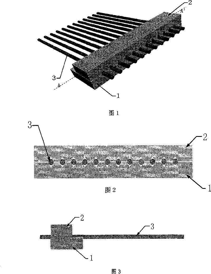
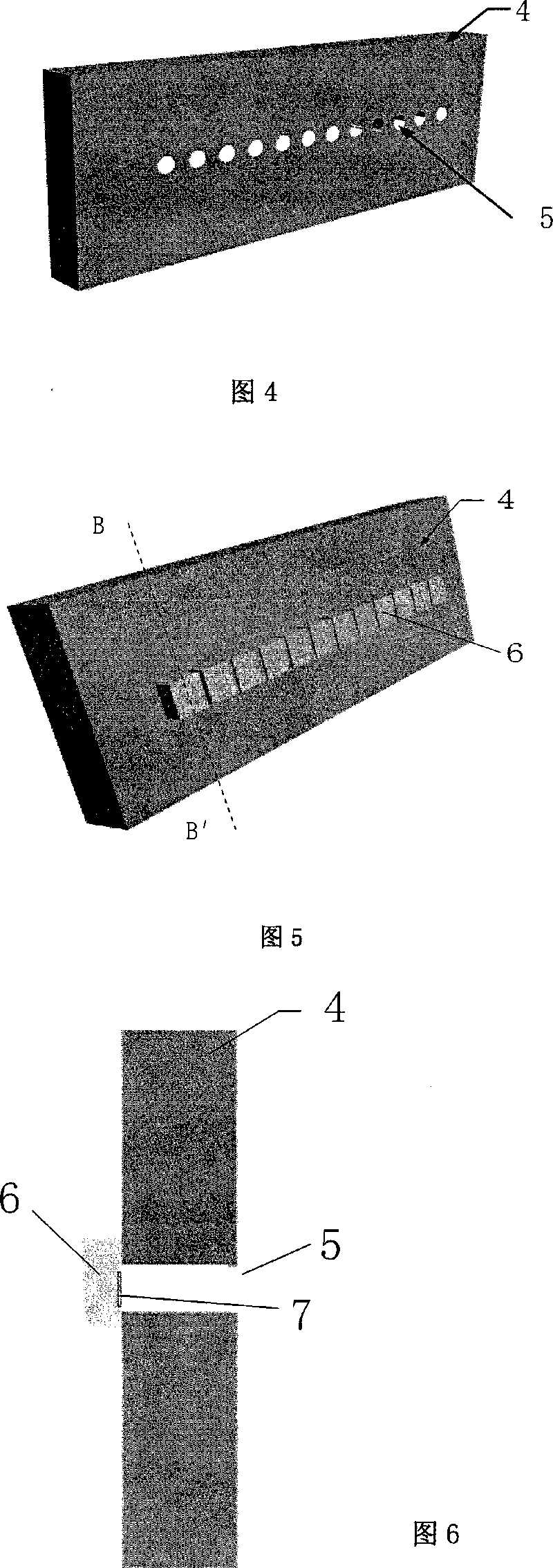
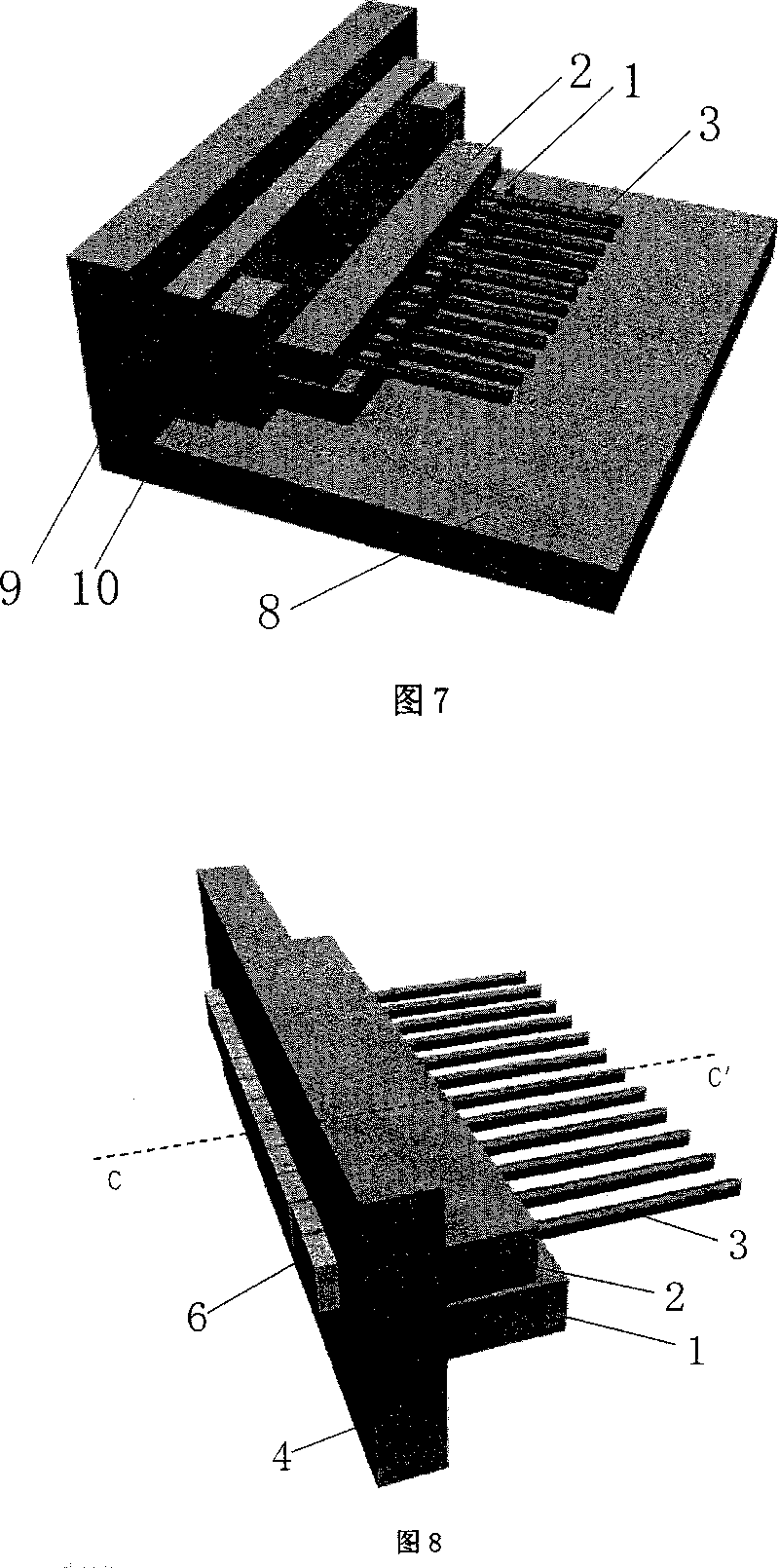
[0042] The invention provides a passive coupling method of an optoelectronic device array and an optical fiber array, especially a surface-emitting or surface-receiving optoelectronic device array, such as a vertical cavity surface-emitting laser VCSEL and a surface-receiving PIN photodetector array, and a multi-mode Passive coupling method between fiber arrays. The micro-via array that penetrates the entire silicon wafer from one side of the silicon wafer is deeply etched and used as the introduction and positioning holes of the optical fiber array. The central axis of each corresponding micro-through hole in the micro-through-hole array is vertically aligned, and the optical fiber array is inserted into the micro-throug...


PUM


Abstract

The invention relates to the field of optical coupling encapsulation technology of photodevice matrix in the optical communication technique and discloses a passive coupling method of photodevice matrix and an optical fiber array; the method comprises the following steps: deep etching is carried out on one side of a substrate to form a micro through hole array penetrating the whole substrate; thephotodevice matrix is arranged in a back-off way on the other side of the substrate, and an active area of each tube core of the photodevice matrix vertically aligns with a central axis of each microthrough hole; and the optical fiber array is inserted into the micro through hole array and fixed. The invention simultaneously discloses a device for preparing the optical fiber array and a method thereof. The passive coupling method provided by the invention is characterized by precise position, high coupling efficiency and simple realizing technique.

Description

technical field [0001] The invention relates to the technical field of optical coupling packaging of optoelectronic device arrays in optical communication technology, in particular to a passive coupling method of optoelectronic device arrays and optical fiber arrays and the preparation of components thereof. Specifically, the present invention relates to a surface-emitting or surface-receiving optoelectronic device array, such as a vertical cavity surface-emitting laser (VCSEL) and a surface-receiving photodetector (PIN) array, and a passive coupling method between a multimode fiber array, And the preparation method of the multimode optical fiber array positioning component used for the input or output light coupling of the photoelectric device array. Background technique [0002] With the development of optical communication networks, especially optical fiber access networks and fiber-to-the-home, and the increasing data transmission volume between large-capacity switching ...

Claims


Application Information

Patent Timeline
Patent Type & Authority Patents(China)
IPC IPC(8): G02B6/42G02B6/26H04B10/12H04B10/25
Inventor 李宝霞万里兮
Owner 上海国增知识产权服务有限公司
Why Eureka
Try Eureka