Printed circuit board
A technology for printed circuit boards and signal layers, applied in the directions of printed circuits, printed circuits, electrical components, etc., can solve the problems of low wiring density of printed circuit boards, less and less volume, and large wiring space.
- Summary
- Abstract
- Description
- Claims
- Application Information
AI Technical Summary
Problems solved by technology
Method used
Image

Examples
Embodiment Construction
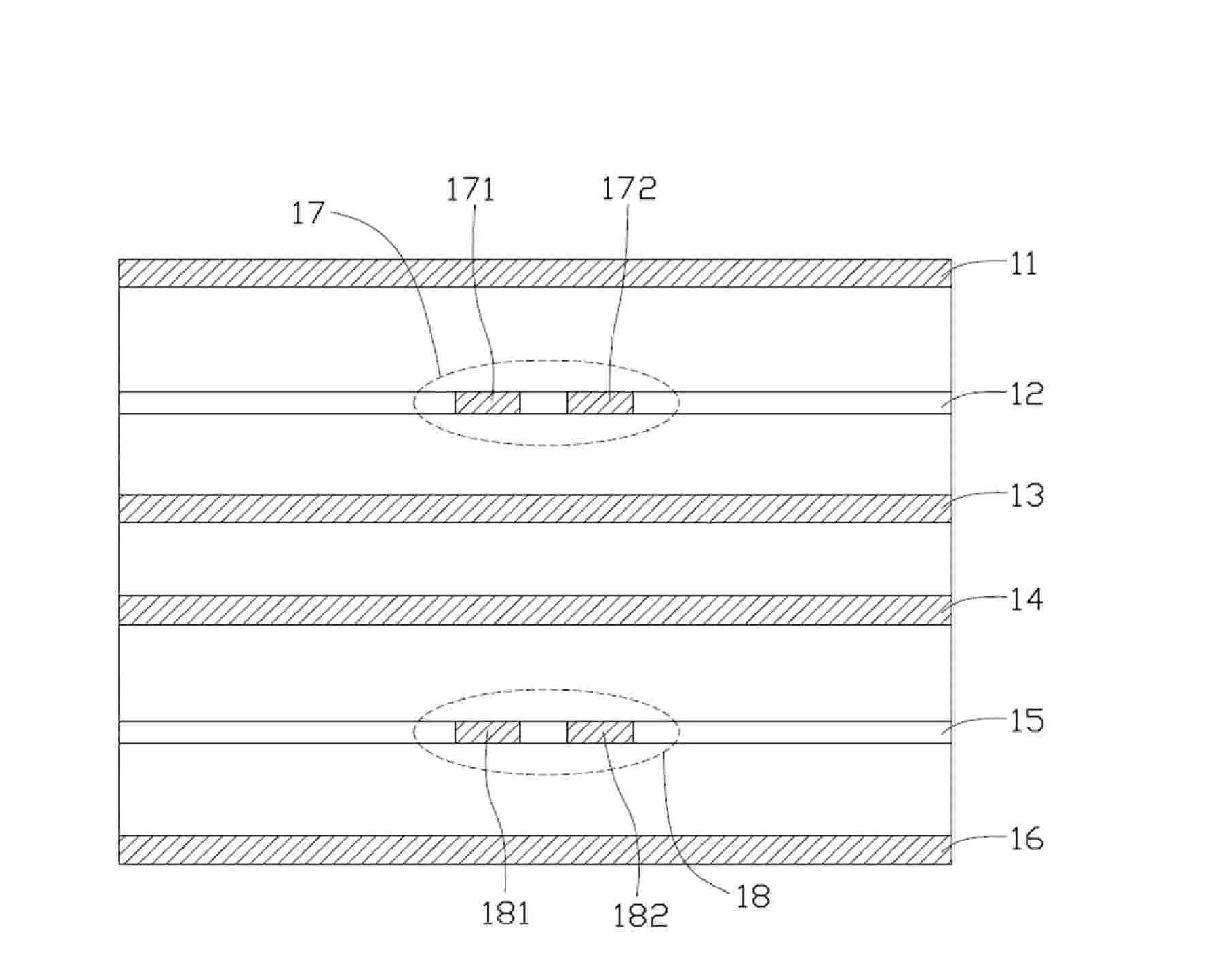
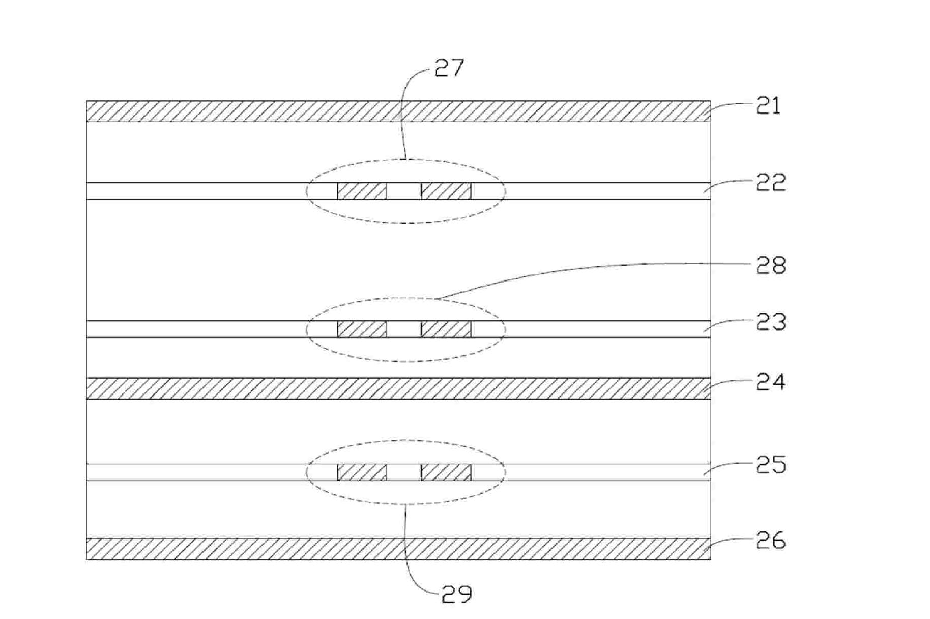
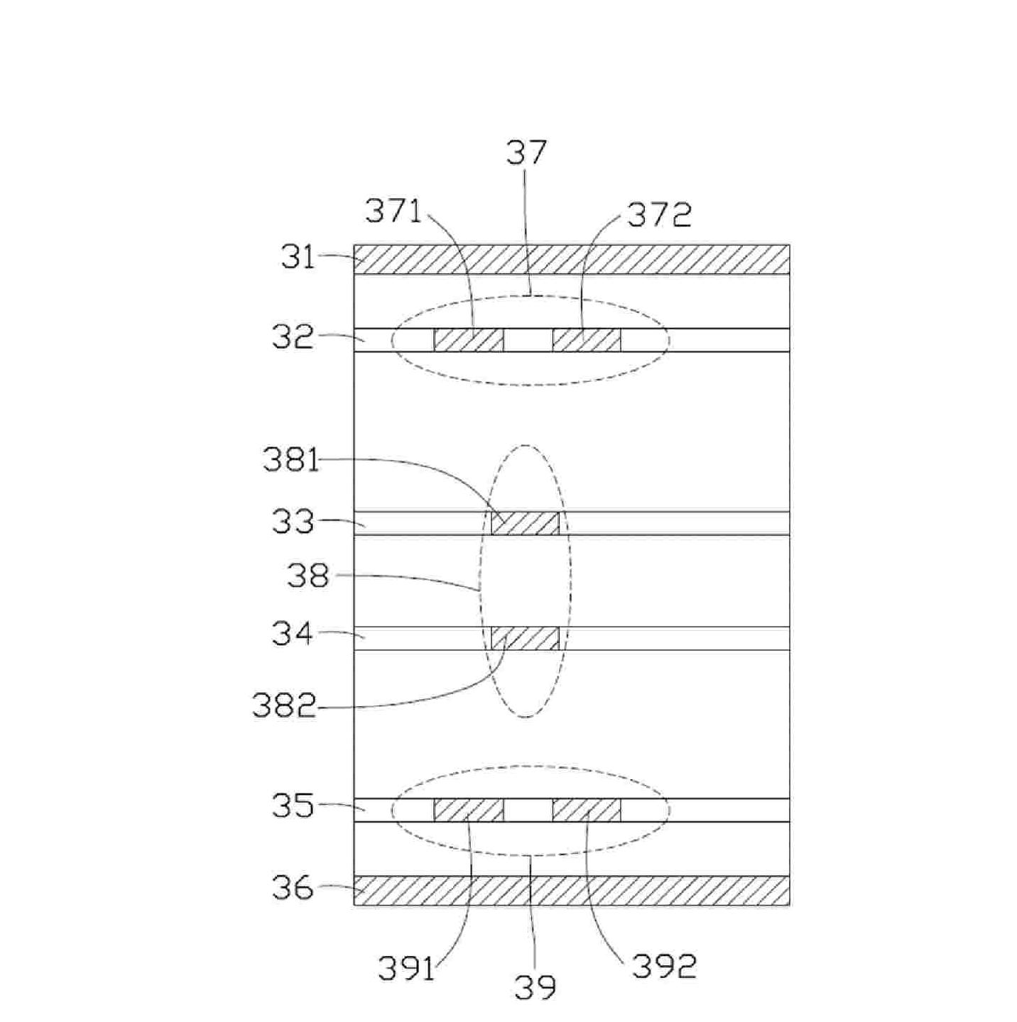
[0012] Please refer to image 3 , The first preferred embodiment of the printed circuit board of the present invention includes a first reference layer 31, a first signal layer 32, a second signal layer 33, a third signal layer 34, and a fourth signal layer 35 stacked and a second reference layer 36 . The first reference layer 31 and the second reference layer 36 can be ground layers or power layers. A differential pair 37 is arranged on the first signal layer 32 in an edge-coupling manner, and the differential pair 37 includes two differential transmission lines 371 and 372 . A differential pair 38 is arranged on the second signal layer 33 and the third signal layer 34 in a broadside-couple manner. The broadside coupling means that two differential transmission lines in a differential pair are coupled between two adjacent layers of the printed circuit board. The differential pair 38 includes two differential transmission lines 381 and 382 , the differential transmission li...
PUM
 Abstract
Description
Claims
Application Information