Formation of multisegmented plated through holes

a technology of multi-segmented plated through holes and forming methods, which is applied in the direction of resistive material coating, printed circuit assembling, metallic material coating processes, etc., can solve the problem of limiting the wiring density that can be achieved in the pcb, and achieve the effect of facilitating an increase in the wiring density of the substra

Inactive Publication Date: 2005-04-14
IBM CORP
View PDF21 Cites 17 Cited by
  • Summary
  • Abstract
  • Description
  • Claims
  • Application Information

AI Technical Summary

Benefits of technology

[0024] The present invention provides a method and structure for utilizing a PTH in a substrate in a manner that facilitates an increased wiring density in the substrate.

Problems solved by technology

Unfortunately, constraining the electrical coupling of such conductive structure to the first and second portions of the PTH limits the wiring density that can be achieved in the PCB.

Method used


Image

  • Formation of multisegmented plated through holes
  • Formation of multisegmented plated through holes
  • Formation of multisegmented plated through holes

Examples


Embodiment Construction

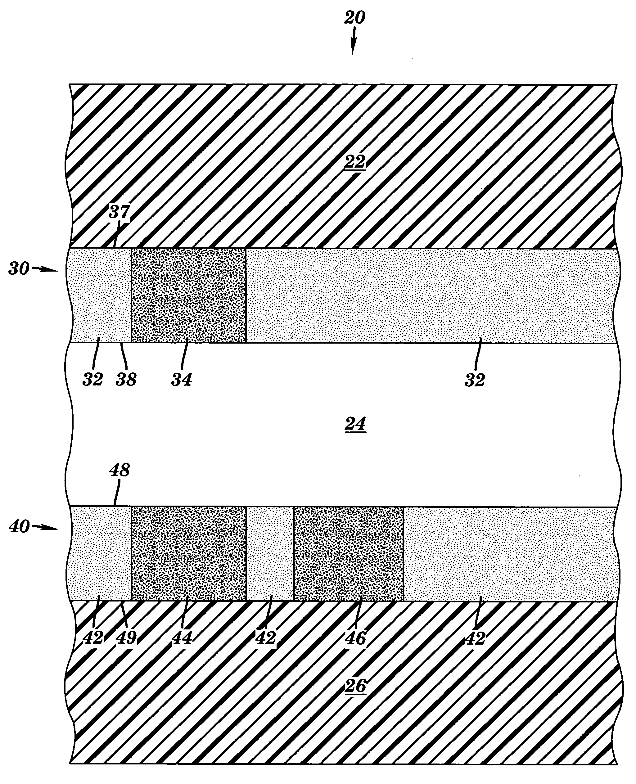
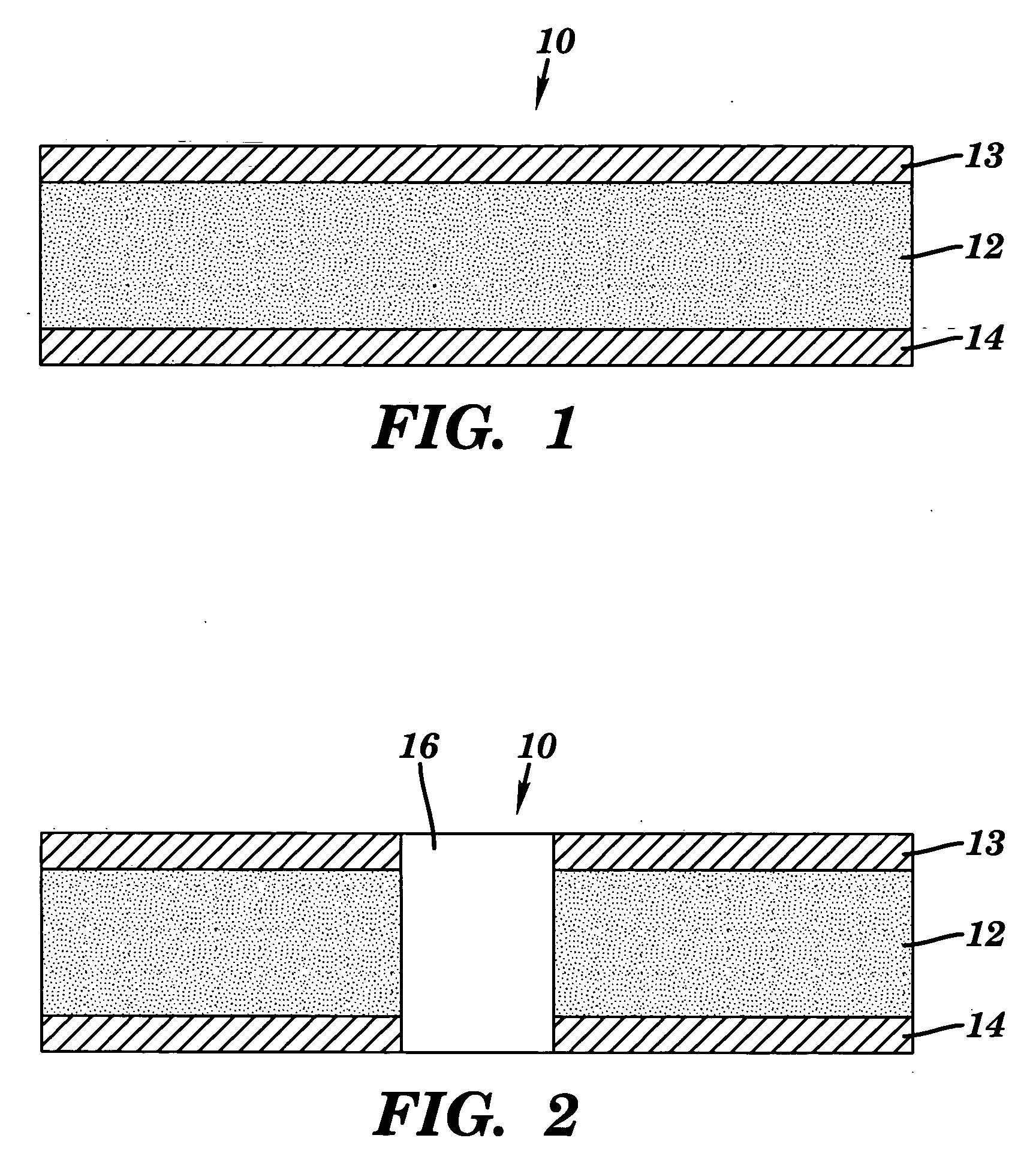
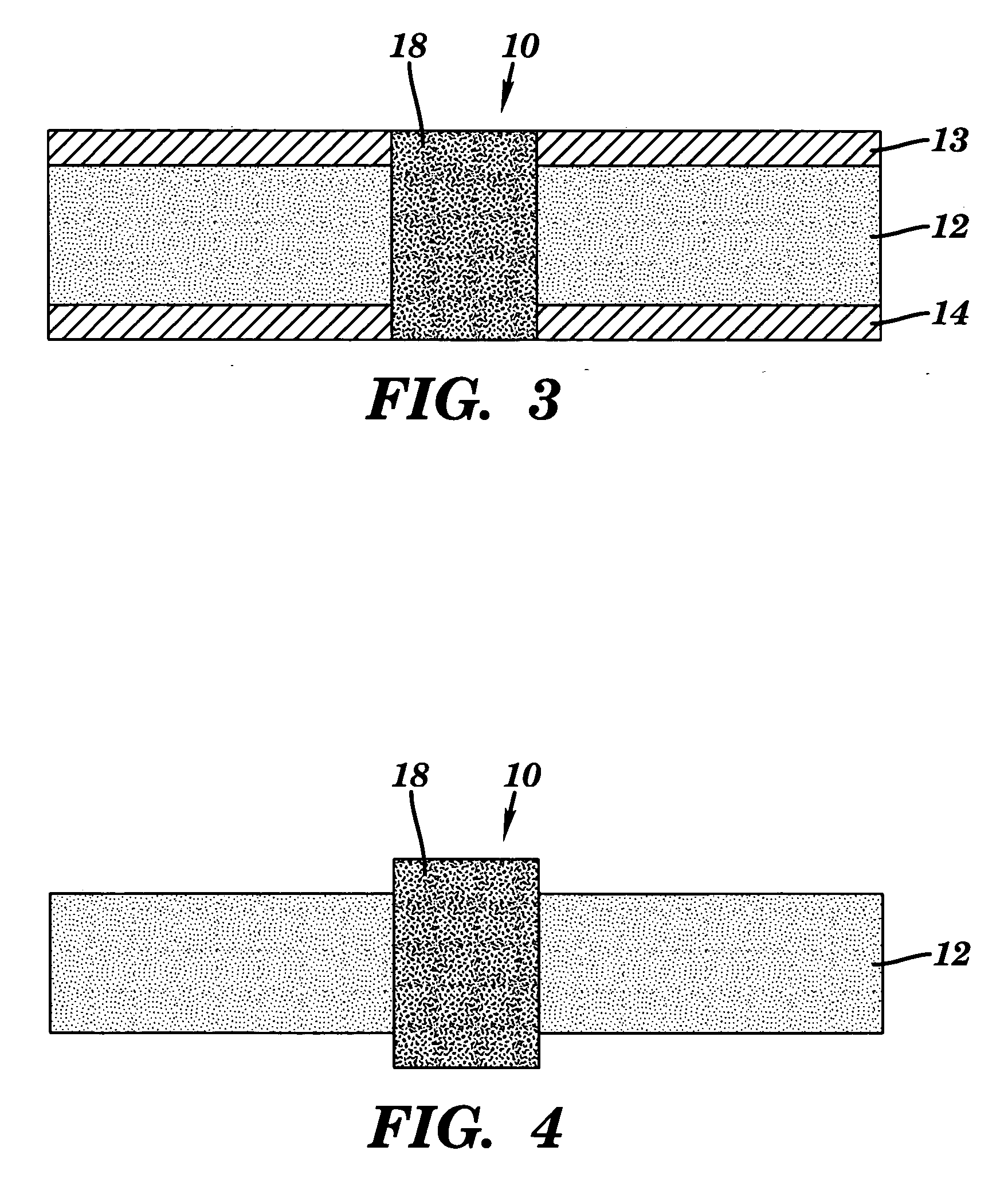
[0040] Embodiments of the present invention are disclosed herein. First embodiments are depicted in FIGS. 1-9. Second embodiments are depicted in FIGS. 10-15.

[0041] In relation to the first embodiments of the present invention, FIG. 1 illustrates a front cross-sectional view of a selective plate core (SPC) 10 in an initial stage of its formation. The SPC 10 comprises a nonplatable dielectric layer 12 sandwiched between metal layers 13 and 14, in accordance with embodiments of the present invention. The metal layers 13 and 14 may each include, inter alia, copper. The nonplatable dielectric layer 12 includes a nonplatable dielectric material that is nonplatable with respect to a seeding process and an electrically conductive metal plating process. That is, the nonplatable dielectric material cannot be electroplated by the seeding process followed by electroplating by the electrically conductive plating process, for any reason including the following two reasons. The first reason is t...


PUM

PropertyMeasurementUnit
surface energyaaaaaaaaaa
dielectricaaaaaaaaaa
densityaaaaaaaaaa

Abstract

A method and structure relating to multisegmented plated through holes. A substrate includes a dielectric layer sandwiched between a first laminate layer and a second laminate layer. A through hole is formed through the substrate. The through hole passes through nonplatable dielectric material within the dielectric layer. As a result, subsequent seeding and electroplating of the through hole results in a conductive metal plating forming at a wall of the through hole on a segment of the first laminate layer and on a segment of the second laminate layer, but not on the nonplatable dielectric material of the dielectric layer. Thus, the conductive metal plating is not continuous from the first laminate layer to the second laminate layer.

Description

BACKGROUND OF THE INVENTION [0001] 1. Technical Field [0002] The present invention relates to plated through holes and more particularly to a method and structure for forming multisegmented plated through holes. [0003] 2. Related Art [0004] A plated through hole (PTH) in a printed circuit board (PCB) provides electrical communication between a first electrically conductive structure electrically coupled to a first portion of the PTH and a second electrically conductive structure electrically coupled to a second portion of the PTH. Unfortunately, constraining the electrical coupling of such conductive structure to the first and second portions of the PTH limits the wiring density that can be achieved in the PCB. [0005] There is a need to utilize a PTH in a substrate in a manner that facilitates increased wiring density in the PCB. SUMMARY OF THE INVENTION [0006] The present invention provides a method for forming at least one multisegmented plated through hole (PTH) in a substrate, c...

Claims


Application Information

Patent Timeline
Patent Type & Authority Applications(United States)
IPC IPC(8): H05K3/42
CPCH05K3/429H05K2201/0187H05K2201/096Y10T428/24917Y10T29/49126Y10T29/49165Y10T29/49155H05K2201/09645
Inventor FARQUHAR, DONALD S.JAPP, ROBERT M.LAUFFER, JOHN M.PAPATHOMAS, KONSTANTINOS I.
Owner IBM CORP
Why Eureka
Try Eureka