Wiring board with embedded component and integrated stiffener and method of making the same

a technology of embedded components and wiring boards, applied in the field of wiring boards, can solve the problems of poor warping control, difficult to embed electronic devices in wiring boards without suffering high yield loss, and other features such as design flexibility are not addressed

Inactive Publication Date: 2017-01-19
BRIDGE SEMICON
View PDF6 Cites 15 Cited by
  • Summary
  • Abstract
  • Description
  • Claims
  • Application Information

AI Technical Summary

Benefits of technology

[0011]The method of making a wiring board according to the present invention has numerous advantages. For instance, inserting the sacrificial carrier and the electronic component into the through opening of the stiffener before the formation of the second routing circuitry is particularly advantageous as the sacrificial carrier together with the stiffener provides a stable platform for forming the second routing circuitry. Forming the encapsulant on the first routing circuitry can provides another high modulus anti-warping platform for the wiring board, so that the warping after removal of the sacrificial carrier can be suppressed by the mechanical robustness of the encapsulant and the stiffener. Additionally, the two-stage formation of the interconnect substrate can avoid serious warping problem when multiple layers of routing circuitries are needed.

Problems solved by technology

However, in addition to poor warping control, other features such as design flexibility are not addressed.
Additionally, it is extremely difficult to embed an electronic device in a wiring board without suffering high yield loss.
This is because minor dislocation of the embedded device due to placement accuracy or adhesive curing dislocation may lead to I / O disconnection, device failure and low manufacturing yield as described in U.S. Pat. Nos. 8,536,715 and 8,501,544.

Method used


Image

  • Wiring board with embedded component and integrated stiffener and method of making the same
  • Wiring board with embedded component and integrated stiffener and method of making the same
  • Wiring board with embedded component and integrated stiffener and method of making the same

Examples


embodiment 1

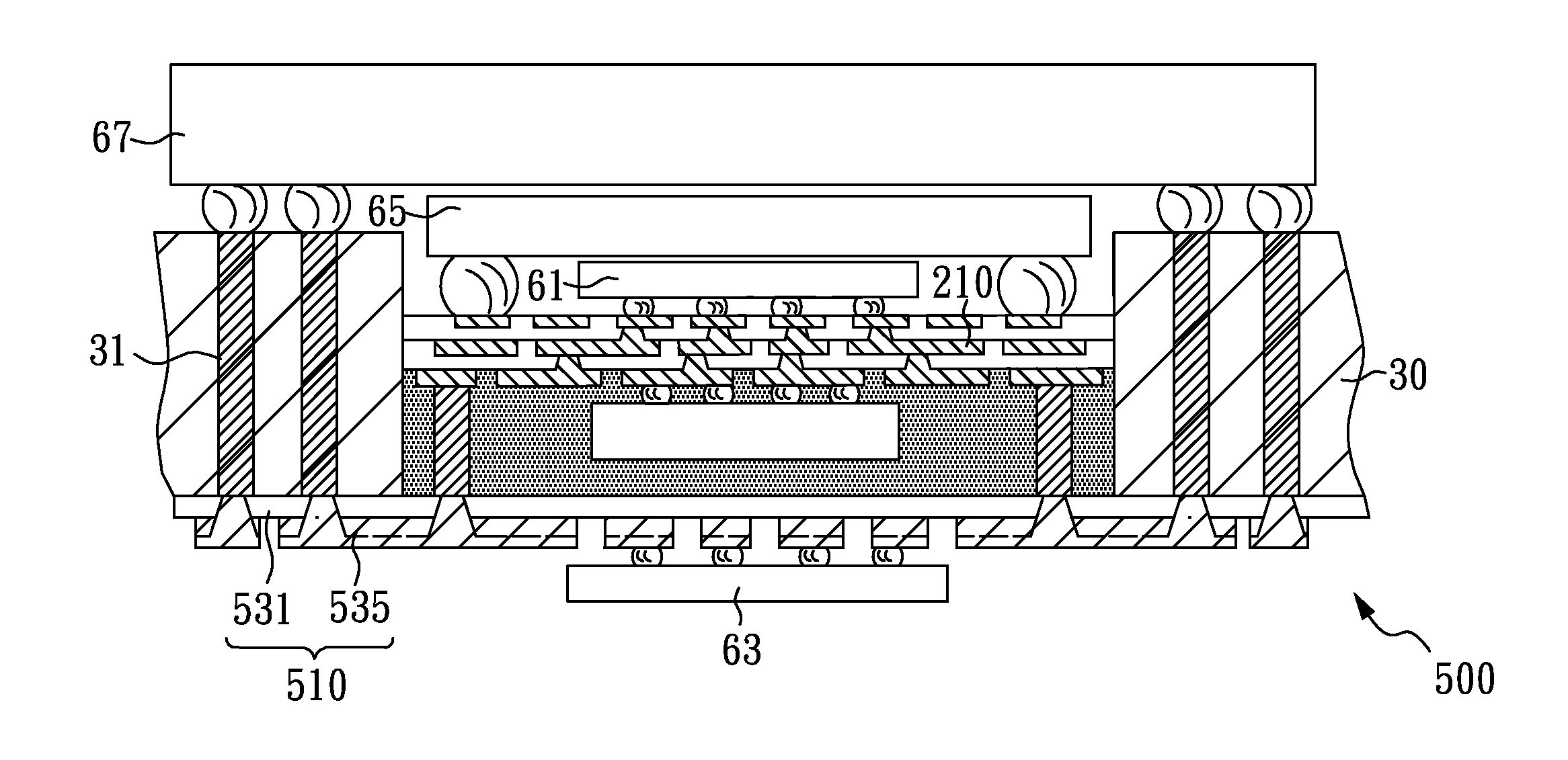
[0059]FIGS. 1-18 are schematic views showing a method of making a wiring board that includes a stiffener, a first routing circuitry, a first semiconductor device, an array of vertical connecting elements, an encapsulant and a second routing circuitry in accordance with the first embodiment of the present invention.

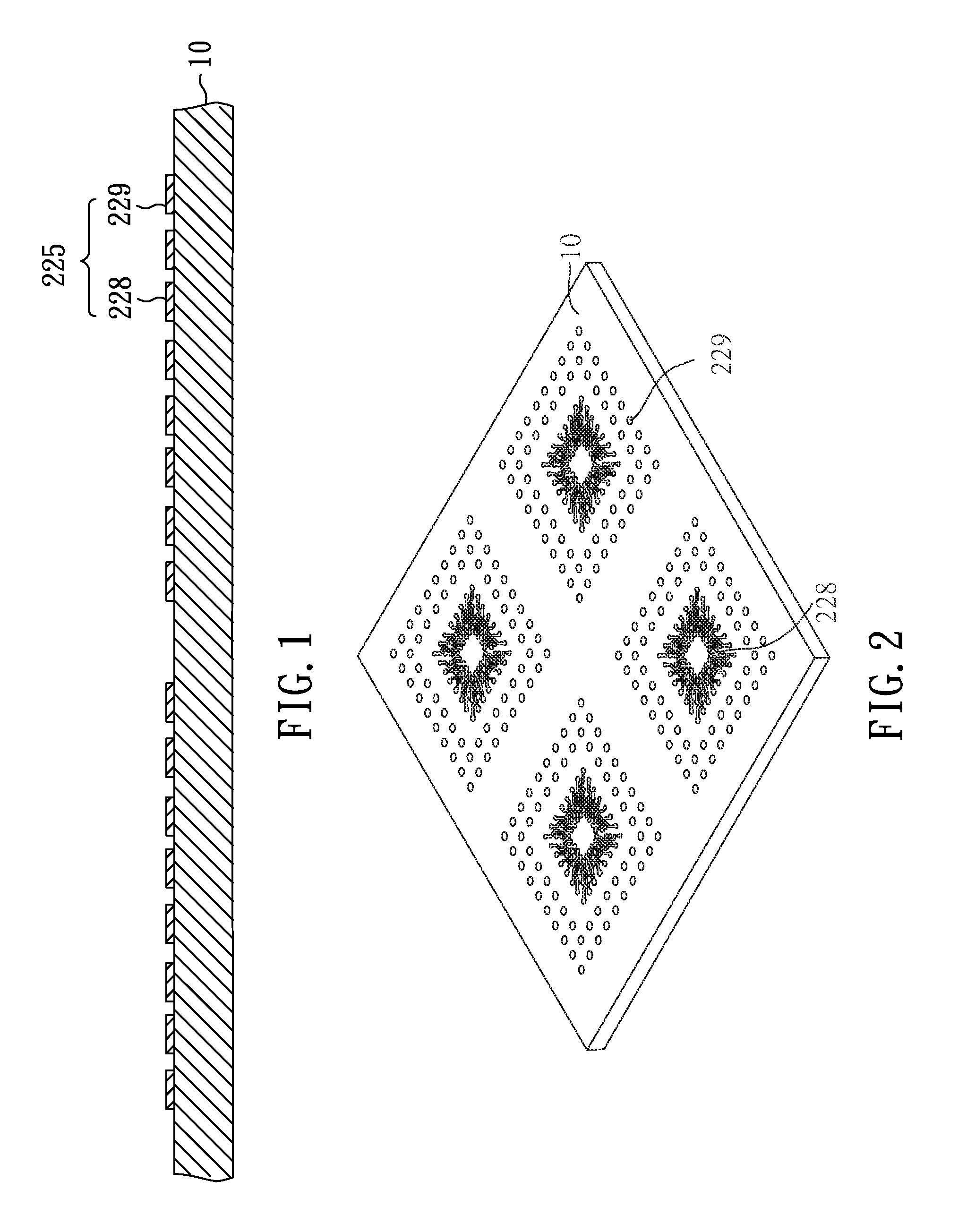
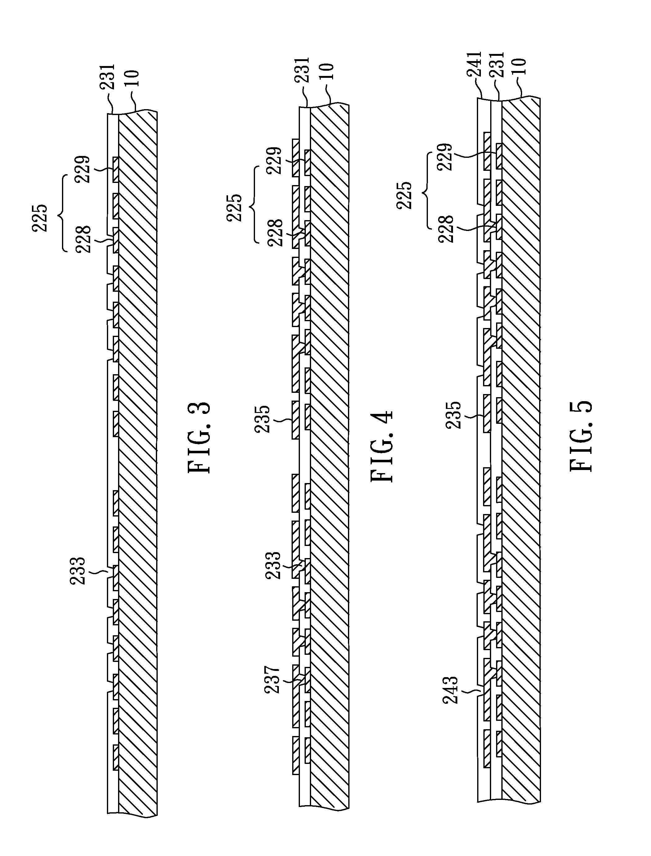
[0060]FIGS. 1 and 2 are cross-sectional and top perspective views, respectively, of the structure with routing traces 225 formed on a sacrificial carrier 10 by metal deposition and metal patterning process. In this illustration, the sacrificial carrier 10 is a single-layer structure, and the routing traces 225 include bond pads 228 and stacking pads 229. The sacrificial carrier 10 typically is made of copper, aluminum, iron, nickel, tin, stainless steel, silicon, or other metals or alloys, but any other conductive or non-conductive material also may be used. The thickness of the sacrificial carrier 10 preferably ranges from 0.1 to 2.0 mm. In this embodiment, the sacrificia...

embodiment 2

[0086]FIGS. 20-30 are schematic views showing a method of making a wiring board having conductive vias as the vertical connecting elements in accordance with the second embodiment of the present invention.

[0087]For purposes of brevity, any description in Embodiment 1 above is incorporated herein insofar as the same is applicable, and the same description need not be repeated.

[0088]FIG. 20 is a cross-sectional view of the structure with a first routing circuitry 210 detachably adhered over a sacrificial carrier 10. The structure, having the first routing circuitry 210 on the sacrificial carrier 10, is similar to that illustrated in FIG. 6, except that the sacrificial carrier 10 is a double-layer structure in this embodiment. The sacrificial carrier 10 includes a support sheet 111 and a barrier layer 113 deposited on the support sheet 111, and the first routing circuitry 210 is formed on the barrier layer 113. The barrier layer 113 can have a thickness of 0.001 to 0.1 mm, and may be a...

embodiment 3

[0103]FIGS. 32-40 are schematic views showing a method of making a wiring board with a heat spreader attached to the first semiconductor device in accordance with the third embodiment of the present invention.

[0104]For purposes of brevity, any description in Embodiments above is incorporated herein insofar as the same is applicable, and the same description need not be repeated.

[0105]FIG. 32 is a cross-sectional view of the structure with a heat spreader 29 attached on the first semiconductor device 26 of FIG. 8. The heat spreader 29 can be made of any material with high thermal conductivity, such as metal, alloy, silicon, ceramic or graphite. The heat spreader 29 is attached on an inactive surface of the first semiconductor devices 26 using a thermally conductive adhesive (not shown in the figure).

[0106]FIG. 33 is a cross-sectional view of the structure with an encapsulant 28 on the first routing circuitry 210, the vertical connecting elements 25 and the heat spreader 29. The encap...


PUM


Abstract

A wiring board with embedded component and integrated stiffener is characterized in that an embedded semiconductor device, a first routing circuitry, an encapsulant and an array of vertical connecting elements are integrated as an electronic component disposed within a through opening of a stiffener, and a second routing circuitry is disposed beyond the through opening of the stiffener and extends over the stiffener. The mechanical robustness of the stiffener can prevent the wiring board from warping. The embedded semiconductor device is electrically coupled to the first routing circuitry and surrounded by the vertical connecting elements in electrical connection with the first and second routing circuitries. The first routing circuitry provides primary fan-out routing for another semiconductor device to be assembled on the wiring board, whereas the second routing circuitry not only provides further fan-out wiring structure, but also mechanically binds the electronic component with the stiffener.

Description

CROSS REFERENCE TO RELATED APPLICATIONS[0001]This application is a continuation-in-part of U.S. application Ser. No. 14 / 746,792 filed Jun. 22, 2015, which claims the priority benefit of U.S. Provisional Application Ser. No. 62 / 092,196 filed Dec. 15, 2014 and the priority benefit of U.S. Provisional Application Ser. No. 62 / 121,450 filed Feb. 26, 2015. The entirety of each of said applications is incorporated herein by reference.FIELD OF THE INVENTION[0002]The present invention relates to a wiring board and, more particularly, to a wiring board having an embedded component and an integrated stiffener, and a method of making the same.DESCRIPTION OF RELATED ART[0003]Market trends of multimedia devices demand for faster and slimmer designs. One of the approaches is to embed an electronic device in a wiring board so that the electrical performance of the board can be improved and / or another device(s) can be assembled on the board to form a 3D stacking structure. U.S. Pat. Nos. 8,453,323, ...

Claims


Application Information

Patent Timeline
Patent Type & Authority Applications(United States)
IPC IPC(8): H01L23/538H01L25/065H01L21/52H01L21/56H01L23/367H01L23/00H01L23/31H01L21/683
CPCH01L23/5389H01L23/5384H01L23/5386H01L23/3121H01L25/0657H01L21/6835H01L2225/06517H01L23/3675H01L23/562H01L21/52H01L2225/06548H01L2225/06589H01L2221/68359H01L21/56H01L21/486H01L21/561H01L21/568H01L23/3677H01L23/4334H01L23/49816H01L23/49822H01L23/49827H01L23/5385H01L24/73H01L24/81H01L24/97H01L2224/16225H01L2224/73204H01L2224/73253H01L2224/81005H01L2224/81203H01L2224/81205H01L2224/81815H01L2224/97H01L2924/00014H01L2924/15311H01L2924/15321H01L2924/181H05K1/181H05K1/183H05K3/4682H05K3/4694H01L25/065Y02P70/50H01L2224/81H01L2224/13099H01L2924/00012
Inventor LIN, CHARLES W. C.WANG, CHIA-CHUNG
Owner BRIDGE SEMICON
Why Eureka
Try Eureka