Silicon chip mark, implementing and reading method thereof

A realization method and marking technology, applied in character and pattern recognition, instruments, electrical components, etc., can solve problems such as error-prone, low efficiency, cumbersome work, etc., and achieve the effect of eliminating mistakes and improving production efficiency

Active Publication Date: 2009-03-18
SHANGHAI HUAHONG GRACE SEMICON MFG CORP
View PDF0 Cites 1 Cited by
  • Summary
  • Abstract
  • Description
  • Claims
  • Application Information

AI Technical Summary

Problems solved by technology

[0003] There are two defects of this kind of silicon wafer marking: one is that it needs to manually read the marking to realize the tracking of the silicon wafer, which is cumbersome, inefficient and prone to mistakes ; The second is that the automatic recognition of the mark cannot be realized, so that the automatic tracking of the silicon wafer cannot be realized

Method used


Image

  • Silicon chip mark, implementing and reading method thereof
  • Silicon chip mark, implementing and reading method thereof
  • Silicon chip mark, implementing and reading method thereof

Examples


Embodiment Construction

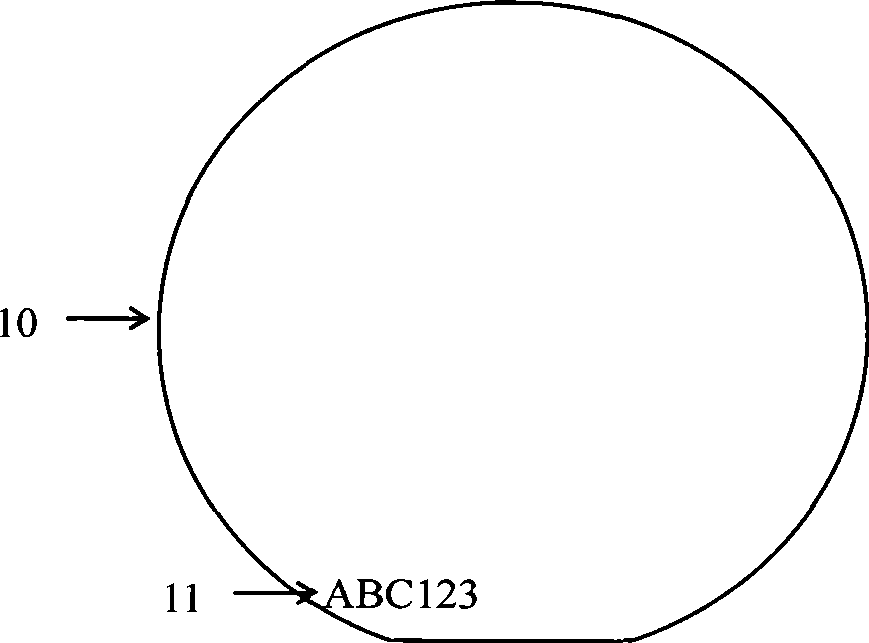
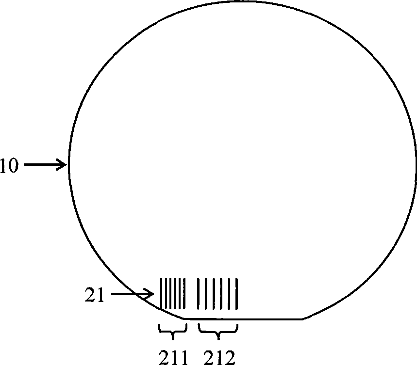
[0018] see figure 2 , the silicon wafer mark of the present invention is a mark 21 formed on the surface of the silicon wafer 10, and the mark 21 is one or more gratings, figure 2 Two gratings 211 and 212 are shown schematically. The present invention requires that the multiple gratings used as the silicon wafer mark 21 have different spatial periods, and these multiple gratings with different spatial periods respectively represent different marking symbols. The so-called marking symbol can be a coded code unit, more commonly Chinese characters, foreign characters or numbers. For example, 26 English letters can be represented by using 26 gratings with different spatial periods, and 10 Arabic numerals can be represented by using 10 gratings with different spatial periods.

[0019] The realization method of the silicon chip mark of the present invention is to form one or more gratings on the surface of the silicon chip. Forming the grating on the surface of the silicon wafe...


PUM


Abstract

The invention discloses a silicon marker, wherein one or a plurality of gratings are formed on the surface of a silicon chip, and the gratings have different spatial cycles which respectively present different mark symbols. The invention further discloses a method for realizing the silicon marker that a plurality of grooves are engraved on the surface of the silicon chip through adopting an engraving device, and the engraved grooves can form one or a plurality of gratings, or a plurality of grooves are formed on the surface of the silicon chip through the photo-etching process and / or the etching process, and the grooves can form one or a plurality of gratings. The invention further discloses a reading method of the silicon marker, which uses laser rays to irradiate one or a plurality of gratings, then identifies the diffraction angle of the diffraction ray of each grating, and finally identifies different mark symbols according to the different diffraction angles. The silicon marker, the realization method and the reading method thereof can realize the automatic identification and tracking for the silicon chip, increase production efficiency, and eliminate failures possibly caused by manual operations.

Description

technical field [0001] The invention relates to marking of silicon wafers in semiconductor manufacturing. Background technique [0002] In semiconductor manufacturing, in order to track silicon wafers, it is necessary to mark the silicon wafers at the beginning of the production line. For commonly used silicon wafer markings, please refer to figure 1 , marking 11 is usually a combination of characters and / or numbers. This silicon chip mark is realized by engraving marks 11 on the surface of the silicon chip 10 . [0003] There are two defects of this kind of silicon chip mark: one is that it needs to manually read the mark to realize the tracking of the silicon chip, which is cumbersome, inefficient and prone to mistakes; Automatic tracking of silicon wafers. Contents of the invention [0004] The technical problem to be solved by the present invention is to provide a silicon wafer mark, which can realize automatic identification of silicon wafers, thereby realizing au...

Claims


Application Information

Patent Timeline
Patent Type & Authority Applications(China)
IPC IPC(8): H01L23/544H01L21/00H01L21/02G06K9/74
Inventor 王雷
Owner SHANGHAI HUAHONG GRACE SEMICON MFG CORP
Why Eureka
Try Eureka