Wide-band antireflective film and optical element with the wide-band antireflective film

An anti-reflection film and optical element technology, applied in optical elements, optics, instruments, etc., can solve the problems of adverse effects on optical performance of optical elements, slight changes in color tone, and poor anti-reflection performance.

Inactive Publication Date: 2009-03-25
HONG FU JIN PRECISION IND (SHENZHEN) CO LTD +1
View PDF0 Cites 13 Cited by
  • Summary
  • Abstract
  • Description
  • Claims
  • Application Information

AI Technical Summary

Problems solved by technology

[0003] The anti-reflection coatings on the current optical components are generally designed for the visible light region, and the anti-reflection performance of infrared light and ultraviolet light that are relatively similar to visible light wavelengths is generally not good.
However, said infrared light or ultraviolet light tends to have a considerable adverse effect on the optical performance of the optical element, for example, if such an optical element is used in a device such as a camera, there may be problems such as slight changes in color tone

Method used


Image

  • Wide-band antireflective film and optical element with the wide-band antireflective film
  • Wide-band antireflective film and optical element with the wide-band antireflective film

Examples


Embodiment Construction

[0010] The present invention will be further described in detail below in conjunction with the accompanying drawings.

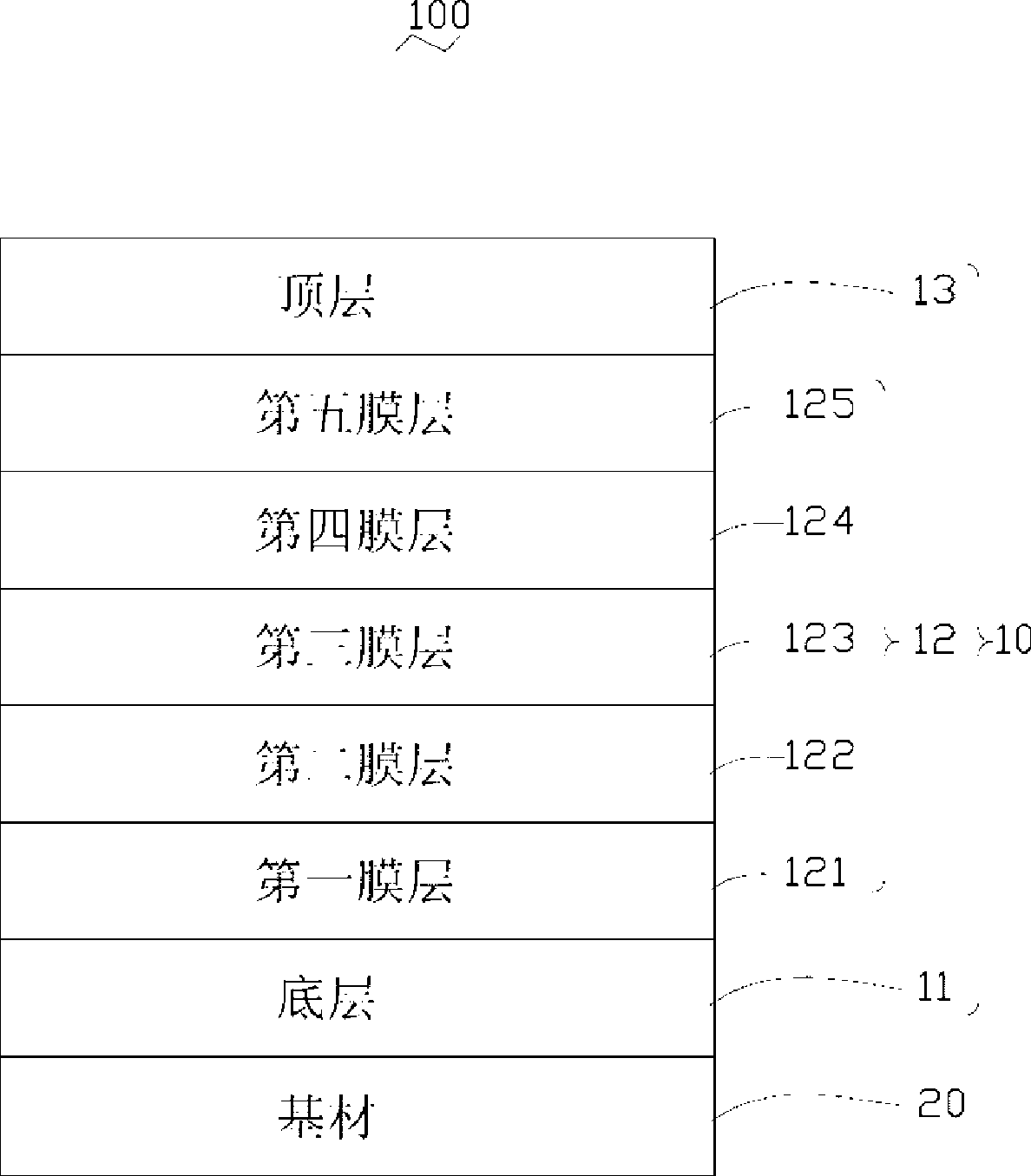
[0011] see figure 1 , is an optical element 100 provided by an embodiment of the present invention, and the optical element 100 includes a substrate 20 and a broadband anti-reflection film 10 formed on one surface of the substrate 20 . The optical element 100 may specifically be an optical element such as a lens or a prism.

[0012] The material of the substrate 20 can be glass or plastic. It can be understood that a broadband anti-reflection film 10 can be formed on each surface of the substrate 20 for light to pass through, such as a lens, which can form a broadband anti-reflection film 10 on both surfaces to improve the lens light transmittance.

[0013] The broadband anti-reflection film 10 includes a bottom layer 11 , a widening layer 12 and a top layer 13 sequentially formed along the surface of the substrate 20 .

[0014] The bottom layer 11 is com...


PUM

PropertyMeasurementUnit
refractive indexaaaaaaaaaa

Abstract

The invention relates to a broadband anti-reflection film, which comprises a bottom layer, a widened layer and a top layer which are formed on the surface of an optical element in turn, wherein the bottom layer is an intermediate refractive index material layer the film thickness of which is between 0.95 and 1.05 d; the top layer is a low refractive index material layer the film thickness of which is between 0.95 and 1.05 d; the widened layer comprises a first film, a second film, a third film, a fourth film and a fifth film which are formed along the direction from the bottom layer to the top layer in turn; the first film is a high refractive index material layer the film thickness of which is between 0.311 and 0.343 d; the second film is a low refractive index material layer the film thickness of which is between 0.147 and 0.163 d; the third film is a high refractive index material layer the film thickness of which is between 1.561 and 1.725 d; the fourth film is a low refractive index material layer the film thickness of which is between 0.210 and 0.232 d; and the fifth film is a high refractive index material layer the film thickness of which is between 0.321 and 0.355 d, wherein d is equal to lambda / (4n), wherein lambda refers to the wavelength of incident light and n refers to the refractive index of a corresponding film.

Description

technical field [0001] The invention relates to an anti-reflection film, in particular to a broadband anti-reflection film and an optical element with the broadband anti-reflection film. Background technique [0002] At present, most of the optical components used in cameras and other imaging devices, such as lenses and prisms, are deposited on the incident or outgoing surfaces of optical components such as lenses and prisms in order to prevent the light attenuation of the incident light when the light passes through. . [0003] The current anti-reflection coatings on optical components are generally designed for the visible light region, and generally have poor anti-reflection performance for infrared light and ultraviolet light that are close in wavelength to visible light. However, the infrared light or ultraviolet light often has a considerable adverse effect on the optical performance of the optical element. For example, if such an optical element is used in a device s...

Claims


Application Information

Patent Timeline
Patent Type & Authority Applications(China)
IPC IPC(8): G02B1/11
CPCG02B1/115
Inventor 林君鸿
Owner HONG FU JIN PRECISION IND (SHENZHEN) CO LTD
Why Eureka
Try Eureka