Vacuum molding device for nanometer stamping

A technology of vacuum molding and nano-imprinting, which is applied in the direction of photoplate-making process, optics, and opto-mechanical equipment on the pattern surface, and can solve the problems of affecting the imprinting accuracy, low degree of automation, and inability to accurately guarantee the imprinting force, etc. , to achieve the effect of ensuring precision

Inactive Publication Date: 2009-03-25
SHANGHAI JIAO TONG UNIV
View PDF0 Cites 4 Cited by
  • Summary
  • Abstract
  • Description
  • Claims
  • Application Information

AI Technical Summary

Problems solved by technology

[0005] Both of the above-mentioned two technologies use manual rotation to apply imprinting force, which is not highly automated and cannot accurately guarantee the imprinting force, which affects the imprinting accuracy; and these two devices both use the method of converting rotational motion For threaded connections with linear motion, at least the template also rotates, and precise positioning cannot be ensured

Method used


Image

  • Vacuum molding device for nanometer stamping
  • Vacuum molding device for nanometer stamping

Examples


Embodiment Construction

[0020] The embodiments of the present invention are described in detail below in conjunction with the accompanying drawings: this embodiment is implemented on the premise of the technical solution of the present invention, and detailed implementation methods and specific operating procedures are provided, but the protection scope of the present invention is not limited to the following the described embodiment.

[0021] The polymer processed in this embodiment is a traditional photoresist—PMMA (polymethyl methacrylate).

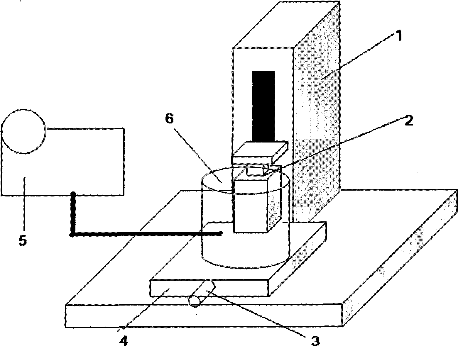
[0022] Such as figure 1 , 2 As shown, this embodiment includes: a tensile testing machine 1, a precision mold fixing system 2, a temperature control system 3, a base 4, a vacuum compressor 5, and a vacuum cover 6, wherein,

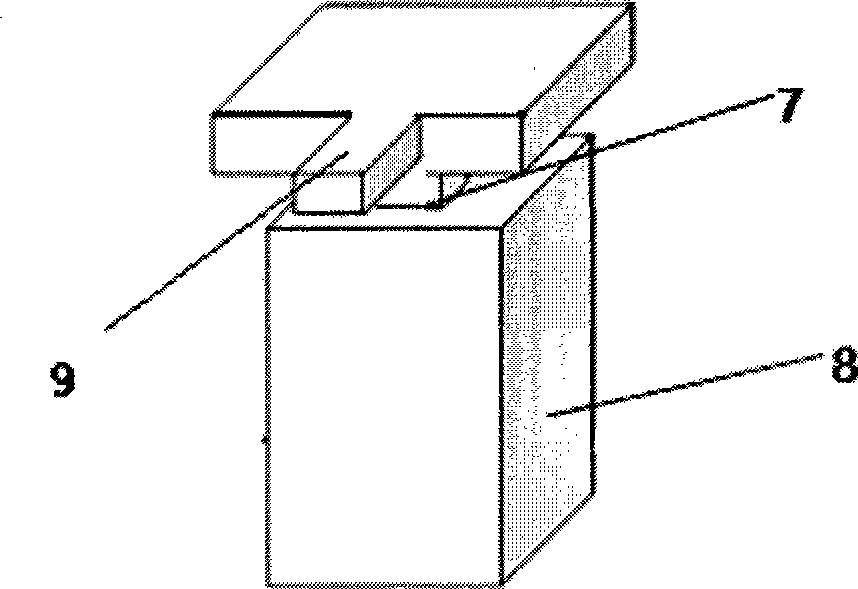
[0023] The vacuum cover 6 is sealed and combined with the base 4, and the vacuum compressor 5 is connected to the vacuum cover 6. The precision mold fixing system 2 is composed of a piston 7 and a guide rail 8. The piston 7 passes throu...


PUM


Abstract

The present invention discloses a vacuum die stamping device for nanometer stamping, which belongs to the technical field of material preparation. The device comprises a tensile testing machine, a precise mold fixing system, a temperature control system, a substrate, a vacuum compressor and a vacuum hood, wherein the vacuum hood is hermetically combined with the substrate; the vacuum compressor is communicated with the vacuum hood; the precise mold fixing system consists of a piston and a guide rail; the piston slides upward and downward in the guide rail; the piston is connected with a driving device in the tensile testing machine and can be slide along a sliding chute of the tensile testing machine; one side of the guide rail is fixed on a housing of the tensile testing machine, while the other side passes through the sidewall of the vacuum hood and is sealed with the vacuum hood; a gap is reserved between the bottom of the guide rail and the substrate for placing a silicon die; and the temperature control system is fixed on the substrate to be in charge of the temperature control inside the vacuum hood. The device causes the nanometer stamping process to be precisely and smoothly completed, and the maximum resolving capability of the stamped pattern can reach 20 nanometers.

Description

technical field [0001] The invention relates to a device in the technical field of material preparation, in particular to a vacuum molding device for nanoimprinting. Background technique [0002] Nanoimprint technology was proposed by Professor S.Y.Chou of Princeton University in 1995. The specific principle is as follows: the polymer is spin-coated on the substrate, and then the template and the substrate are loaded and clamped on two platens on the stamping machine. The polymer is usually a conventional photoresist such as PMMA (polymethyl methacrylate). The graphics are then transferred by applying pressure. Next, the polymer is cured by nanoimprinting technology. For example: thermal embossing technology, UV nano-imprinting technology, micro-contact printing technology, etc. After demolding and reactive ion etching of the residual polymer on the substrate, the transfer and replication of the microstructure pattern from the template to the substrate is finally realize...

Claims


Application Information

Patent Timeline
Patent Type & Authority Applications(China)
IPC IPC(8): G03F7/00
Inventor 李以贵张冠孙健陈少军
Owner SHANGHAI JIAO TONG UNIV
Why Eureka
Try Eureka