Planar lightwave circuit, manufacturing method thereof, and light waveguide device

A technology of planar light wave and manufacturing method, which is applied in the direction of optical waveguide light guide, coupling of optical waveguide, light guide, etc., can solve the problems of influence, etch time extension, etc.

Inactive Publication Date: 2009-04-01
NEC CORP
View PDF2 Cites 8 Cited by
  • Summary
  • Abstract
  • Description
  • Claims
  • Application Information

AI Technical Summary

Problems solved by technology

As a result, the etching time of the end face 81a of the lower cladding layer 81 is prolonged and thus more susceptible to the reaction product film

Method used


Image

  • Planar lightwave circuit, manufacturing method thereof, and light waveguide device
  • Planar lightwave circuit, manufacturing method thereof, and light waveguide device
  • Planar lightwave circuit, manufacturing method thereof, and light waveguide device

Examples


Embodiment Construction

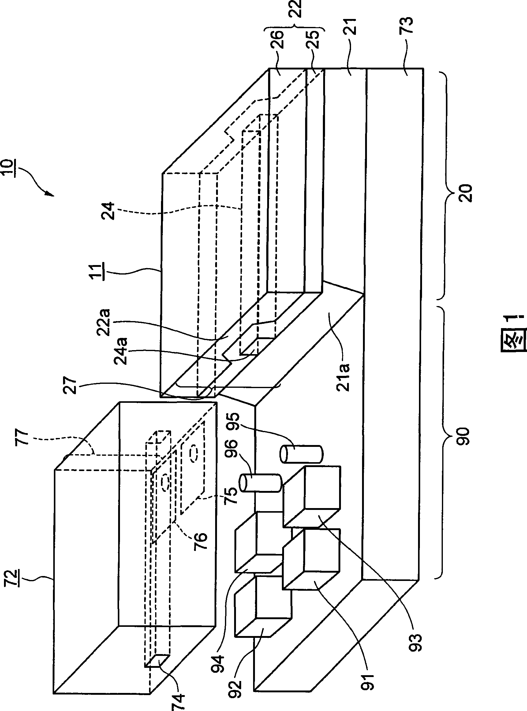
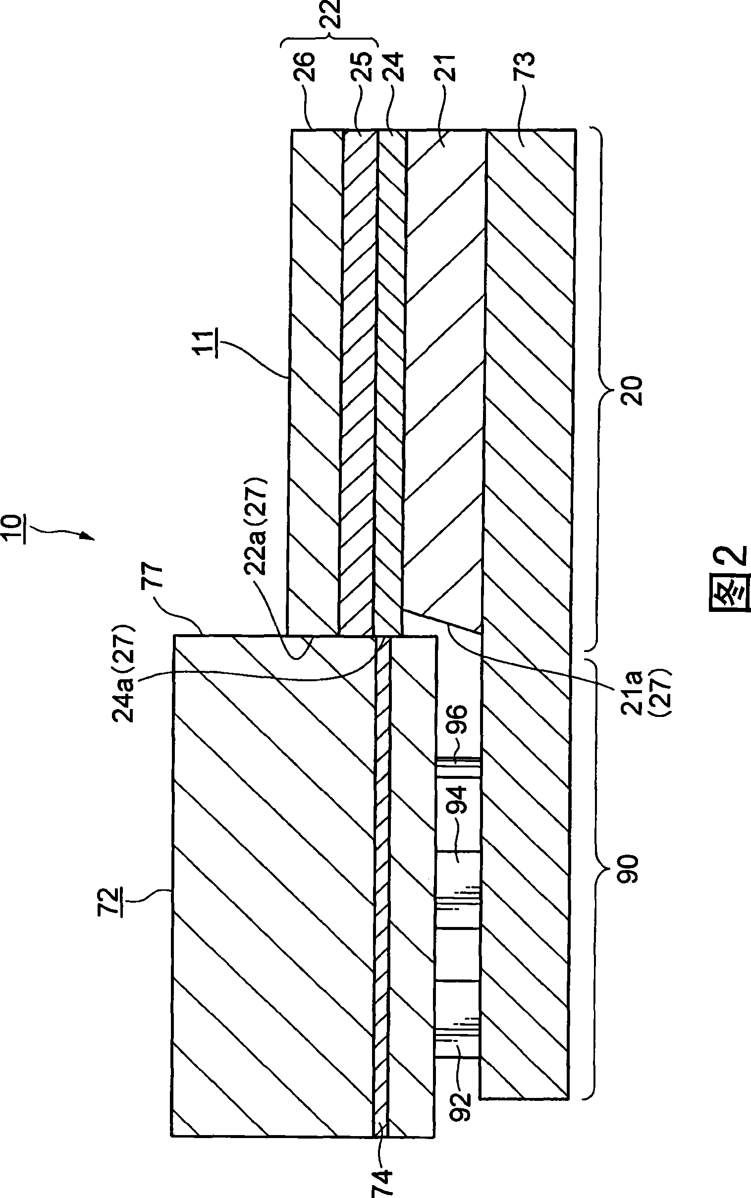
[0023] FIG. 1 is a detailed perspective view showing an exemplary embodiment of an optical waveguide device according to the present invention before packaging. FIG. 2 is a cross-sectional view of the optical waveguide device in FIG. 1 after packaging. Description will be given below with reference to FIGS. 1 and 2 . The same reference numerals are used on the same elements as those in FIGS. 7 and 8 , and explanations thereof are omitted.

[0024] The optical waveguide device 10 according to this exemplary embodiment includes the PLC 11 of the exemplary embodiment and the LD 72 as an optical element mounted on the PLC 11 . The PLC 11 includes an optical waveguide part 20 and an optical element mounting part 90 . The optical waveguide member 20 has a lower cladding layer 21, a core layer 24, and an upper cladding layer 22 formed on a part of a silicon substrate 73 as a substrate. The optical element mounting part 90 has the LD 72 mounted on the silicon substrate 73 , wherein...


PUM


Abstract

To provide a PLC and the like, which can improve the optical coupling efficiency by coupling an optical element to a light waveguide part without having a gap. The PLC includes a light waveguide part and an optical element mount part. The light waveguide part has a lower clad layer, a core layer, and an upper clad layer formed on a part of a silicon substrate as a substrate. The optical element mount part has an LD, which is to be optically coupled at the light waveguide end face as an end face of the light waveguide, loaded on the silicon substrate. At the light waveguide end face, an end face of the lower clad layer is recessed with respect to an end face of the core layer and an end face of the upper clad layer towards a direction away from the LD.

Description

technical field [0001] The present invention relates to a planar optical wave circuit having an optical waveguide member, an optical element mounting member, and the like on a substrate. Hereinafter, "planar lightwave circuit" is referred to as PLC for short. Background technique [0002] As an optical transceiver used on the market in the optical access industry, there are micro-optical device-type modules equipped with LD (laser diode), PD (photodiode), thin-film filter, lens, etc., and by fabricating on a silicon substrate A PLC module composed of a quartz waveguide and LD, PD, etc. installed on its surface. Both types have advantages and disadvantages. However, since the latter does not require adjustment of the optical axis while monitoring the light output, it is advantageous in terms of cost and transportation. The mounting method used in the latter PLC modules is often referred to as passive alignment packaging. Using the passive alignment package, positioning ac...

Claims


Application Information

Patent Timeline
Patent Type & Authority Applications(China)
IPC IPC(8): G02B6/12G02B6/13G02B6/136G02B6/122G02B6/42
CPCG02B6/136G02B6/423G02B6/4219G02B6/4224G02B6/12G02B6/42
Inventor 渡边真也
Owner NEC CORP
Why Eureka
Try Eureka