
Circuit module, wireless communication apparatus and circuit module manufacturing method

A circuit assembly and manufacturing method technology, applied in the direction of printed circuit manufacturing, printed circuit components, circuits, etc., can solve the problems of reducing the productivity of circuit assemblies, obstacles to the productivity of circuit assemblies, etc., and achieve the effect of miniaturization of the overall structure and stable electrical characteristics

Inactive Publication Date: 2009-04-01
KYOCERA CORP
View PDF2 Cites 47 Cited by
  • Summary
  • Abstract
  • Description
  • Claims
  • Application Information

AI Technical Summary

Problems solved by technology

[0014] Furthermore, there is also a problem that it is necessary to prepare a shielding plate 105 of an optimum size in accordance with the size of the metal cover 103 or the size of the semiconductor component 102a, which reduces the productivity of the circuit assembly.
In particular, when a circuit assembly is manufactured using a main substrate having a plurality of substrate regions, the metal cover 103 needs to be attached to each substrate region, and shield plates 105 as many as the metal cover 103 must be prepared. Becomes a big obstacle in improving the productivity of circuit components

Method used


Image

  • Circuit module, wireless communication apparatus and circuit module manufacturing method
  • Circuit module, wireless communication apparatus and circuit module manufacturing method
  • Circuit module, wireless communication apparatus and circuit module manufacturing method

Examples


Embodiment Construction

[0069]

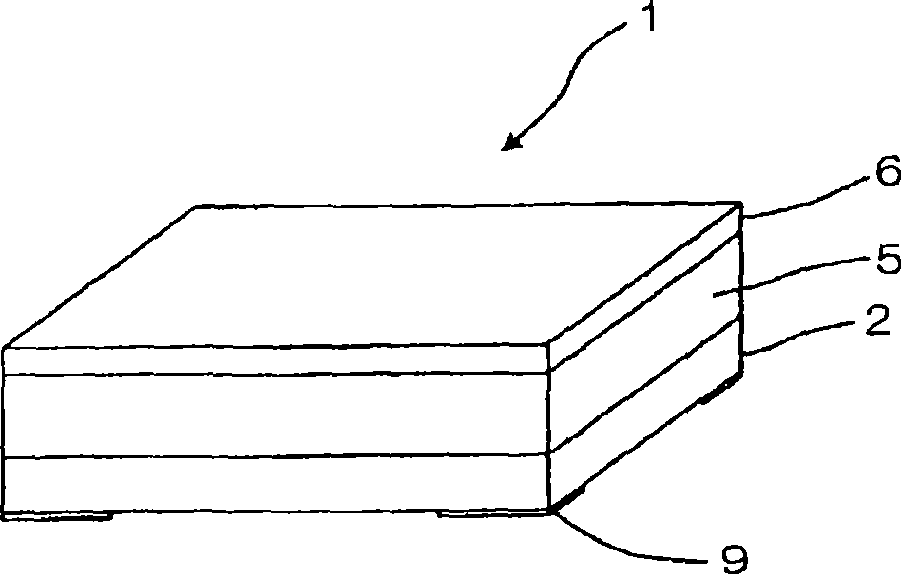
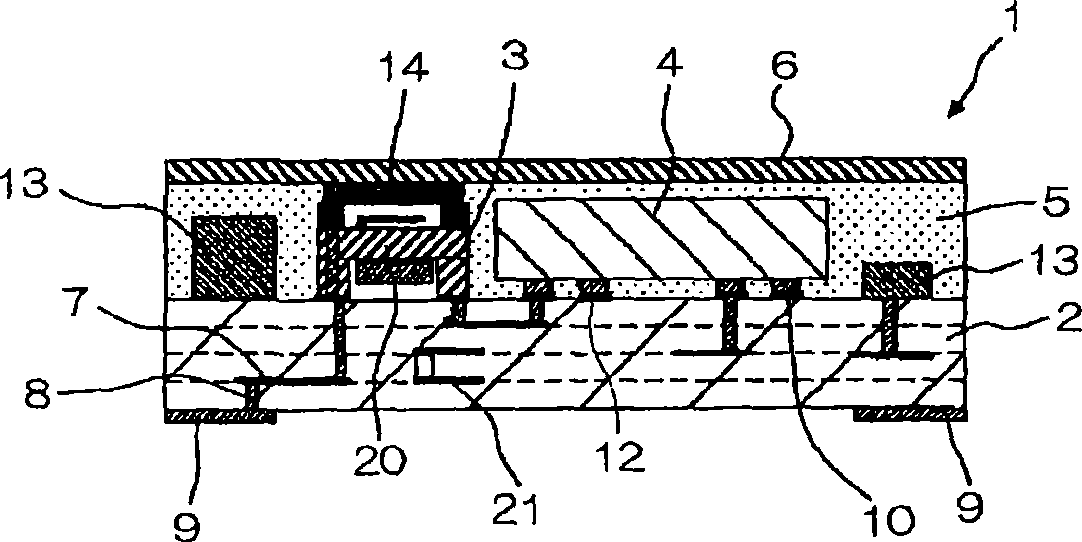
[0070] figure 1 is an external perspective view of a circuit assembly according to an embodiment of the present invention, figure 2 yes figure 1 Cutaway view of the circuit assembly shown.

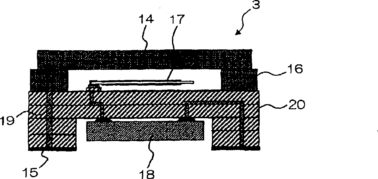
[0071] This circuit module 1 includes a wiring board 2 , a plurality of electronic components arranged and mounted on the wiring board 2 , an insulating resin portion 5 covering the plurality of electronic components, and a conductive layer 6 covering the insulating resin portion 5 . The plurality of electronic components described above include an electronic component 3 with a shielding function and a semiconductor component 4 . In addition, the "electronic component with a shielding function" in this invention means the electronic component which has the function of electromagnetically shielding the element arrange|positioned inside.

[0072] The wiring board 2 is, for example, a substantially cuboid substrate of 7 mm×5 mm×0.4 mm in thickness, and is formed by laminating...


PUM


Abstract

An electronic component (3) which has a shielding function and has the upper surface held at a reference potential, an electronic component (13) and a semiconductor component (4) are mounted on a wiring substrate (2). These components are covered with an insulating resin section (5), and a conductive layer (6) is formed on an upper surface of the insulating resin section (5). The conductive layer (6) is held at the reference potential by connecting the conductive layer (6) with a portion of the electronic component (3), which is held at the reference potential of the electronic component (3) and exposed from the insulating resin section (5). Thus, a small circuit module having excellent electromagnetic shielding function is provided.

Description

technical field [0001] The present invention generally relates to circuit assemblies used in wireless communication devices. Background technique [0002] In recent years, a circuit module configured by mounting a plurality of electronic components including semiconductor components and passive elements on a wiring board has rapidly spread. These circuit components are used, for example, in wireless communication devices such as mobile phones, and have a function of processing high-frequency signals. [0003] In this way, in order to process high-frequency signals, a shielding layer having an electromagnetic shielding function is formed in the circuit assembly to suppress the influence of electromagnetic waves from the outside and prevent unnecessary electromagnetic waves from leaking to the outside. In related circuit components in the past, metal covers are often used as shielding layers. [0004] However, in order to reduce the thickness of circuit components, it is mor...

Claims


Application Information

Patent Timeline
Patent Type & Authority Applications(China)
IPC IPC(8): H01L25/04H01L25/18H03H9/02H03H9/25
CPCH01L2924/09701H05K2201/10492H01L2924/10329H01L2924/01042H01L2224/13025H01L23/66H03H9/1021H01L2224/73253H01L2924/01015H01L2224/16H03H9/0547H01L2224/97H01L2924/01047H01L2224/16225H01L2924/01004H01L25/03H01L2924/01078H01L2924/01006H01L2924/3025H01L2924/19041H01L2924/15192H01L2924/01079H01L2223/6677H01L2924/01074H01L2924/14H05K3/284H01L2924/01005H01L2924/12041H01L2924/01082H01L2924/01013H01L2924/19042H01L23/552H01L25/165H01L2924/30107H05K2201/09972H01L2924/01029H01L24/97H01L2924/19043H03H9/0542H01L2924/01033H05K1/0218H01L2924/01075H01L2224/16235H01L2924/181H01L2924/19105Y10T29/49137H01L2224/81H01L2924/00012
Inventor 畠中英文松尾香
Owner KYOCERA CORP
Learn More