External appearance defect examination method for circuit board

A technology of appearance defects and inspection methods, which is applied in measuring devices, material analysis through optical means, instruments, etc., can solve the problems of difficult quality control of circuit boards, slow inspection speed, inadaptability, etc., and achieve flexibility and scalability Strong performance, fast inspection speed, and high inspection efficiency

Inactive Publication Date: 2009-04-08
GUANGDONG ZHENGYE TECH
View PDF0 Cites 44 Cited by
  • Summary
  • Abstract
  • Description
  • Claims
  • Application Information

AI Technical Summary

Problems solved by technology

[0002] At present, for the final visual inspection of circuit boards, most manufacturers use manual visual inspection, but manual inspection has its inherent defects, so the final quality control of circuit boards is quite difficult. This inspection method not only There are problems of missed inspection and slow inspection speed, and with the advancement of circuit board miniaturization, it is more and more unsuitable

Method used


Image

  • External appearance defect examination method for circuit board

Examples


Embodiment Construction

[0020] In order to facilitate the understanding of those skilled in the art, the present invention will be described in detail below in conjunction with the embodiments and accompanying drawings:

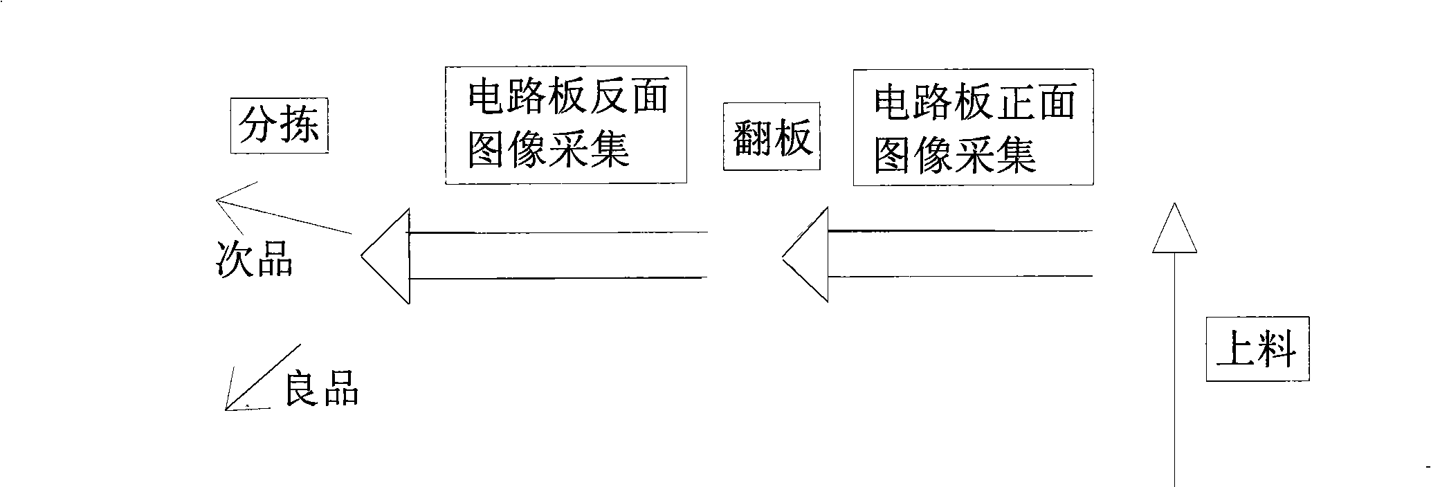
[0021] as attached figure 1 As shown, the method is used for automatic inspection of various defects in the appearance of the circuit board when automatic production is realized. The method includes:

[0022] Loading, image acquisition of the front side of the circuit board, flipping, image acquisition of the reverse side of the circuit board, image analysis, and sorting.

[0023] The loading can be done automatically, and the circuit boards to be inspected are placed on the conveyor belt one by one, and the conveyor belt carries the circuit boards and moves to the scanning device.

[0024] The scanning device is located above the conveyor belt. When the circuit board to be inspected passes through the scanning device, the scanning device scans the image of the front of the circuit...


PUM


Abstract

The invention provides a method used for testing the appearance defects of a circuit board, comprising the steps as follows: loading, collecting frontal images of the circuit board, collecting the reverse images of the circuit board, analyzing and sorting the images. The method can complete the appearance defect check on two surfaces of the circuit board extremely conveniently and quickly, can adopt a computer for automatic control, has quick check speed and high check efficiency, and can check the defects on the circuit board such as foreign matter, exposed copper, supplemented oil, scraping, poor gold-plating, character error, non-uniform green oil, non-uniform welding disc, non-uniform depth of channel, residual copper, omitted printing, developing and the like.

Description

technical field [0001] The invention relates to a circuit board inspection device, in particular to a circuit board appearance defect inspection method. Background technique [0002] At present, for the final visual inspection of circuit boards, most manufacturers use manual visual inspection, but manual inspection has its inherent defects, so the final quality control of circuit boards is quite difficult. This inspection method not only There are problems of missed inspection and slow inspection speed, and with the advancement of circuit board miniaturization, it is becoming more and more unsuitable. In the industry, the demand for fast, highly discriminative, and highly automated devices for visual inspection of circuit boards is increasing. Contents of the invention [0003] The technical problem to be solved by the present invention is to provide a method for inspecting appearance defects of a circuit board. [0004] In order to solve the problems of the technologies...

Claims


Application Information

Patent Timeline
Patent Type & Authority Applications(China)
IPC IPC(8): G01N21/956B07C5/342
Inventor 梅领亮徐地华陈伯平王天辉李伟李能学王树华吴敏邓世文
Owner GUANGDONG ZHENGYE TECH
Why Eureka
Try Eureka