Method and apparatus for growing semiconductor crystals and crystal product and device support method

A product and gas technology, applied in the field of growing semiconductor crystals, devices, crystal products and device supports, can solve the problems of not only providing precise and controlled heating of seed crystal wells, loss, and not being able to solve the requirements of temperature gradient control, etc.

Inactive Publication Date: 2009-04-15
AXT INC +1
View PDF0 Cites 5 Cited by
  • Summary
  • Abstract
  • Description
  • Claims
  • Application Information

AI Technical Summary

Problems solved by technology

In the same way that solid crucible support designs are detrimental to temperature control, techniques based on convective heating with gases or fluids also do not address the specific temperature gradient control requirements of most crystal growth techniques, such as vertical gradient solidification (VGF) techniques
[0012] Conventional solutions based on convection and conduction heating techniques cannot provide both precise and controlled heating of the seed wells and reliable physical stability suitable for high-volume crystal production

Method used


Image

  • Method and apparatus for growing semiconductor crystals and crystal product and device support method
  • Method and apparatus for growing semiconductor crystals and crystal product and device support method
  • Method and apparatus for growing semiconductor crystals and crystal product and device support method

Examples


Embodiment Construction

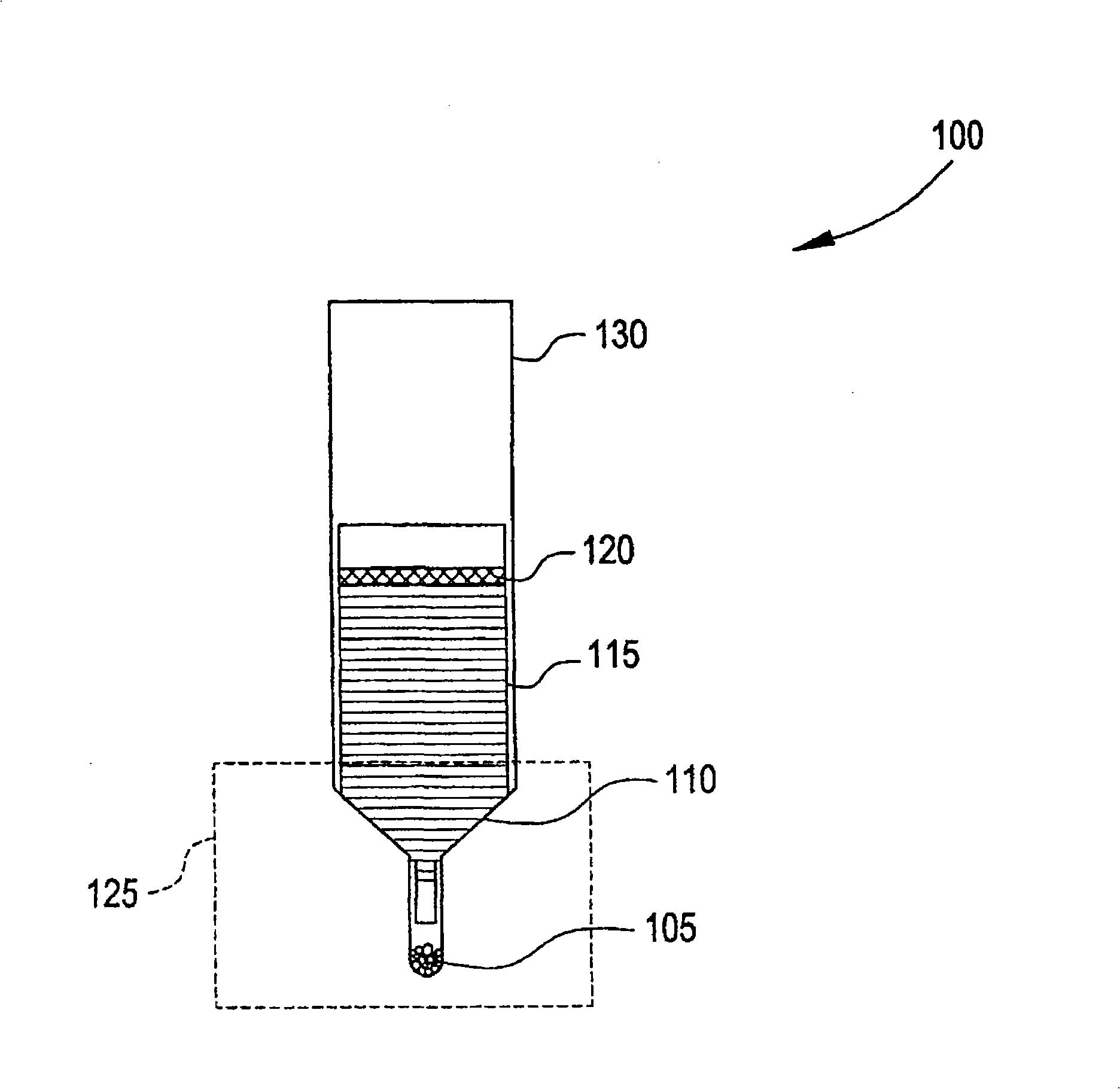
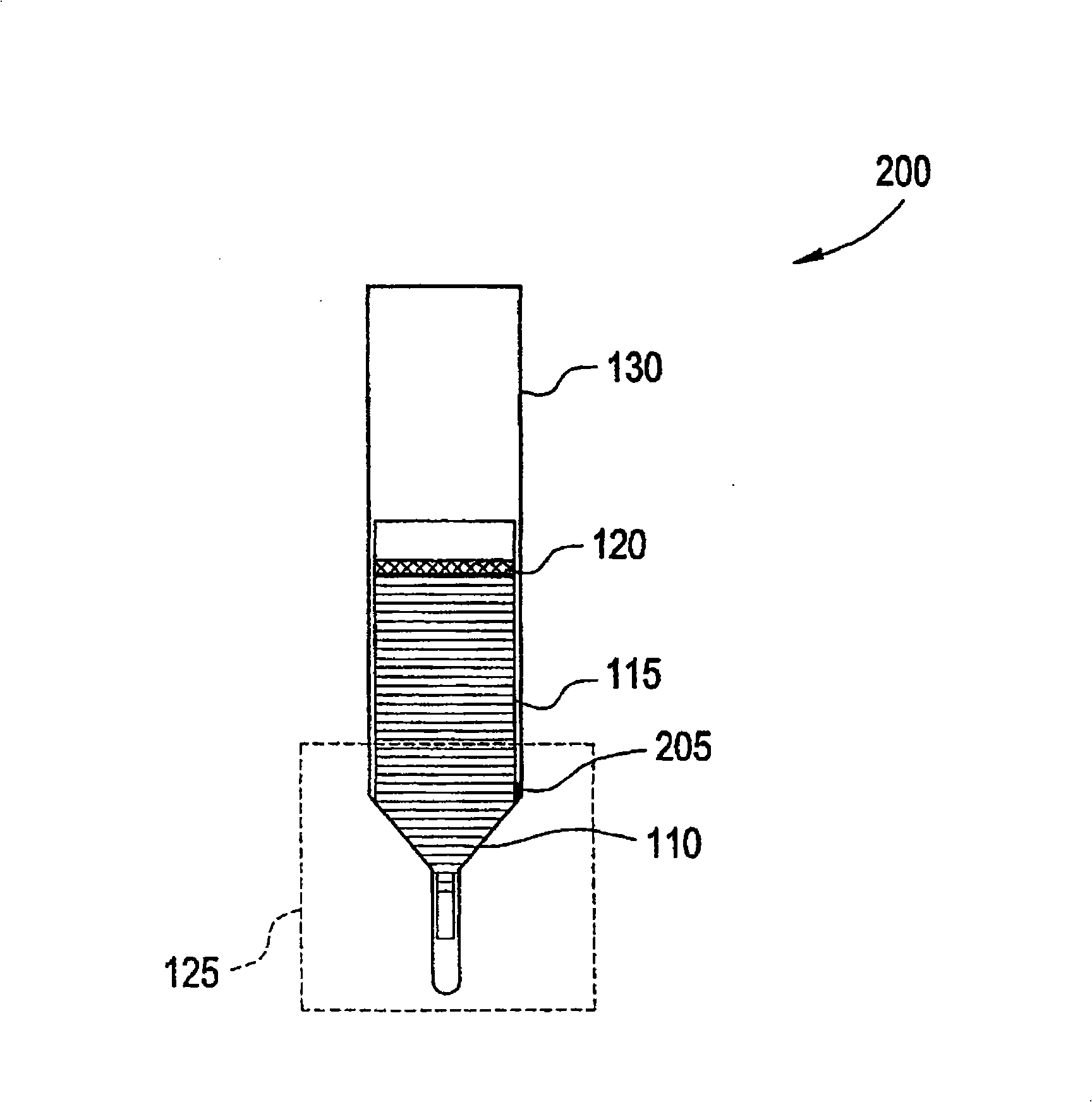
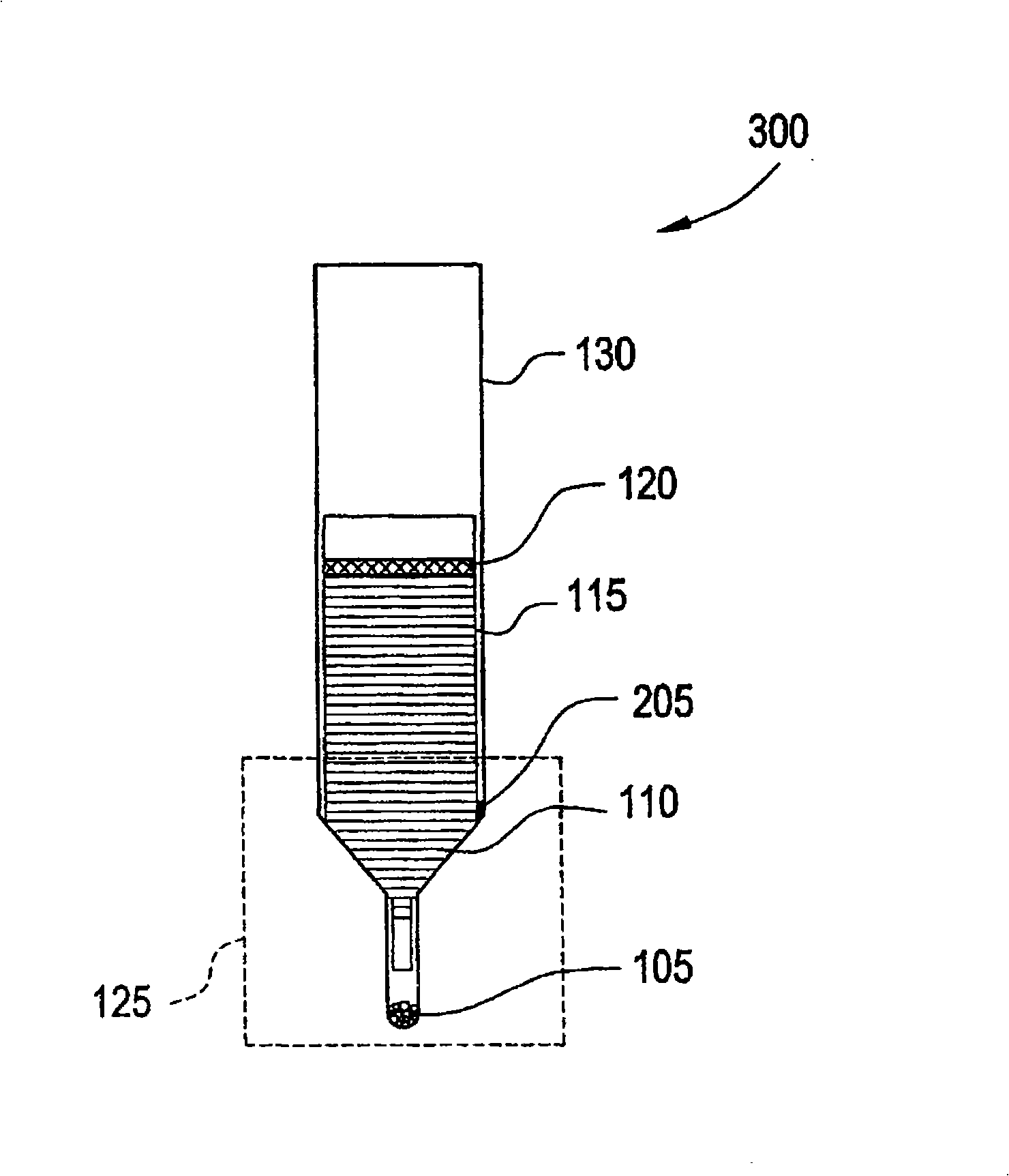
[0022] Exemplary embodiments of the present invention generally involve the growth of III-V, II-VI and related single crystal compounds under conditions with strong supports, doping and resistivity control, and temperature gradients. Using VGF growth of GaAs as an illustrative example, an embodiment of a method of carbon doping and resistivity control in a VGF growth process and an embodiment of a method of setting a crucible support in a VGF growth furnace are described below.

[0023] VGF involves crystal growth technology, equipment and process technology to grow large single crystal ingots with very high structural uniformity and low defect density. In one embodiment, the crystal ingot is substantially cylindrical with a diameter greater than 4 inches and a length greater than 6 inches. This substantially cylindrical crystal grows along a direction perpendicular to the seed crystal, and the seed crystal is under the polycrystalline raw material.

[0024] In one embodiment, the...


PUM

PropertyMeasurementUnit
diameteraaaaaaaaaa
lengthaaaaaaaaaa

Abstract

Group III-V, II-VI and related monocrystalline compounds are grown with a rigid support of a sealed ampoule, carbon doping and resistivity control, and thermal gradient control in a crystal growth furnace. A support cylinder provides structural support for the combined sealed ampoule crucible assembly, while low-density insulating material inside the support cylinder deters convection and conduction heating. Radiation channels penetrating the low-density material provide pathways for radiation heating into out of the seed well and transition regions of the crystal growth crucible. A hollow core in the insulation material directly beneath the seed well provides cooling in the center of the growing crystal, which enables uniform, level growth of the crystal ingot and a flat crystal-melt interface which results in crystal wafers with uniform electrical properties.

Description

[0001] This application is a subdivision of the invention patent No. PCT / US02 / 21195 entitled "Method and device for growing semiconductor crystals with solid support, carbon doping, resistivity control, and temperature gradient control" filed on July 3, 2002. The original application entered the Chinese national phase on February 13, 2004, and obtained the Chinese patent application number 02815865.2. [0002] References to previous applications in this field [0003] This application claims the rights of U.S. Provisional Application No. 60 / 303,189, titled "Non-contact carbon doping and resistivity control in the growth of gallium arsenide", which was filed on July 5, 2001. Technical field [0004] The present invention generally relates to the field of growth of III-V, II-VI and related single crystal compounds, and more specifically, to methods and methods for growing semiconductor crystals with strong supports, carbon doping and resistivity control, and thermal gradient control....

Claims


Application Information

Patent Timeline
Patent Type & Authority Applications(China)
IPC IPC(8): C30B11/04C30B11/14C30B29/42C30B11/00C30B21/02C30B27/00
CPCC30B11/12C30B11/04C30B29/42C30B11/00C30B35/002C30B11/002C30B27/00Y10T117/1092C30B15/20
Inventor X·G·刘W·G·刘
Owner AXT INC
Why Eureka
Try Eureka