Three-dimensional quantum well CMOS integrated device and preparation method thereof

A technology of integrated devices and quantum wells, applied in semiconductor/solid-state device manufacturing, electric solid-state devices, semiconductor devices, etc., can solve the problem of low speed of three-dimensional integrated circuits, and achieve the goal of ensuring AC and DC electrical performance, improving performance, and improving performance Effect

Inactive Publication Date: 2010-06-02
XIDIAN UNIV
View PDF3 Cites 0 Cited by
  • Summary
  • Abstract
  • Description
  • Claims
  • Application Information

AI Technical Summary

Problems solved by technology

[0013] The purpose of the present invention is to provide a kind of three-dimensional quantum well CMOS integrated device and manufacturing method thereof, to solve the problem of low speed of existing three-dimensional integrated circuits

Method used


Image

  • Three-dimensional quantum well CMOS integrated device and preparation method thereof
  • Three-dimensional quantum well CMOS integrated device and preparation method thereof
  • Three-dimensional quantum well CMOS integrated device and preparation method thereof

Examples


Embodiment 1

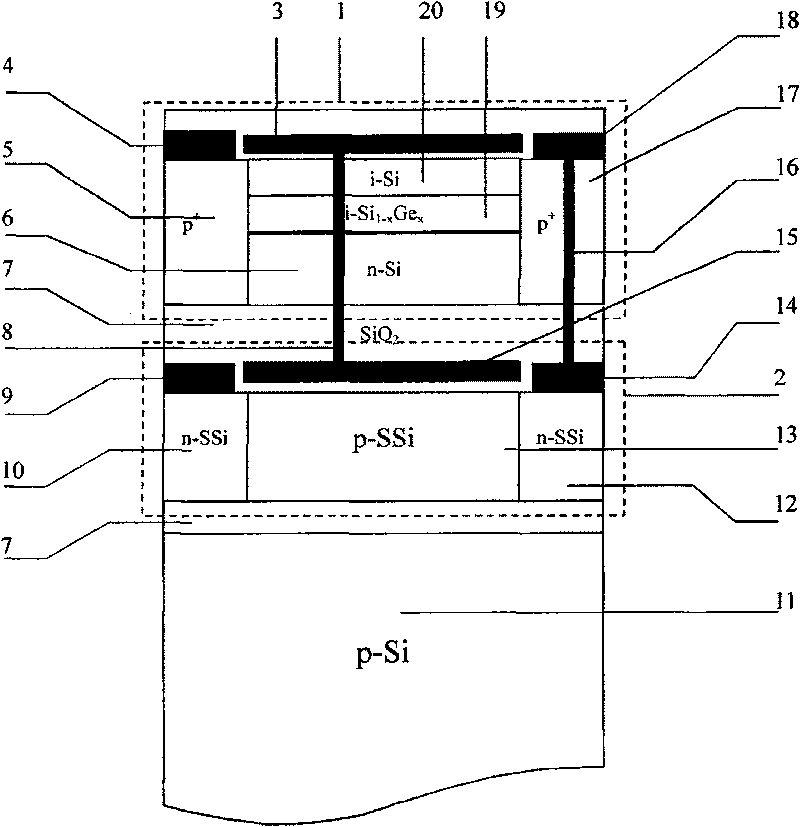
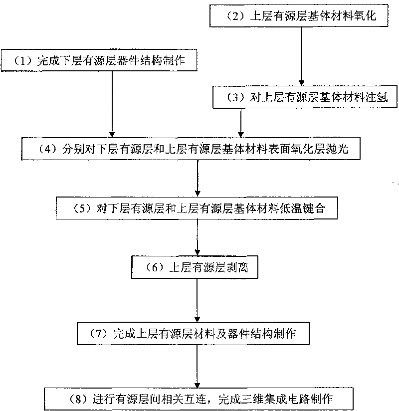
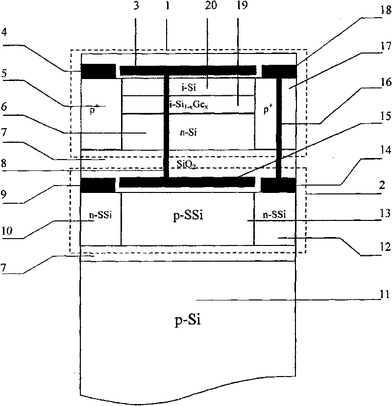
[0040] Embodiment 1: The steps for fabricating a three-dimensional quantum well CMOS integrated device with a 90nm conductive channel are as follows:

[0041] (1) Select SSOI substrate with stress> 1Gpa;

[0042] (2) On the SSOI substrate, use oxidation-photolithography source, drain, gate region-gate oxidation-deposition of polysilicon-photolithography of polysilicon and diffusion layer contact hole-deposition of polysilicon-photolithography of polysilicon-phosphorus implantation-low temperature deposition Product SiO 2 -Lithography lead hole-Polysilicon wiring-Low temperature deposition of SiO 2 Dielectric layer, fabricating strained Si nMOSFET device structure with 90nm conduction channel and interconnecting each other to complete the lower active layer structure;

[0043] (3) Depositing SiO on the surface of the above active layer 2 Dielectric layer

[0044] (4) Surface oxidation of the cleaned n-type Si wafer as the upper base material;

[0045] (5) Use ion implantation process to...

Embodiment 2

[0052] Embodiment 2: The steps for fabricating a three-dimensional quantum well CMOS integrated device with a 130 nm conductive channel are as follows:

[0053] (1) Select SSOI substrate with stress> 1Gpa;

[0054] (2) On the SSOI substrate, use oxidation-photolithography source, drain, gate region-gate oxidation-deposition of polysilicon-photolithography of polysilicon and diffusion layer contact hole-deposition of polysilicon-photolithography of polysilicon-phosphorus implantation-low temperature deposition Product SiO 2 -Lithography lead hole-Polysilicon wiring-Low temperature deposition of SiO 2 Dielectric layer, fabricating strained Si nMOSFET device structure with 130nm conduction channel and interconnecting to complete the lower active layer structure;

[0055] (3) Depositing SiO on the surface of the above active layer 2 Dielectric layer

[0056] (4) Surface oxidation of the cleaned n-type Si wafer as the upper base material;

[0057] (5) Use ion implantation process to implant...

Embodiment 3

[0064] Embodiment 3: The steps of fabricating a three-dimensional quantum well CMOS integrated device with a 65nm conductive channel are as follows:

[0065] (1) Select SSOI substrate with stress> 1Gpa;

[0066] (2) On the SSOI substrate, use oxidation-photolithography source, drain, gate region-gate oxidation-deposition of polysilicon-photolithography of polysilicon and diffusion layer contact hole-deposition of polysilicon-photolithography of polysilicon-phosphorus implantation-low temperature deposition Product SiO 2 -Lithography lead hole-Polysilicon wiring-Low temperature deposition of SiO 2 Dielectric layer, fabricating strained Si nMOSFET device structure with 65nm conduction channel and interconnecting to complete the lower active layer structure;

[0067] (3) Depositing SiO on the surface of the above active layer 2 Dielectric layer

[0068] (4) Surface oxidation of the cleaned n-type Si wafer as the upper base material;

[0069] (5) Use ion implantation process to implant hyd...


PUM


Abstract

The invention discloses a 3D quantum well CMOS integrated device and a manufacturing method thereof, relates to the technical field of microelectronics, and mainly solves the problem of low speed of the existing 3D integrated circuits. The proposal is that an SSOI substrate and an SSGOI substrate are employed to construct two active layers of a new 3D integrated device; wherein, the lower active layer is the SSOI substrate and is made into strained Si nMOSFET by utilizing the characteristic of high electron mobility of a strained Si material in the SSOI substrate; the upper active layer is theSSGOI substrate and is made into strained SiGe quantum well channel pMOSFET by utilizing the characteristic of high hole mobility of a strained SiGe material in the SSGOI substrate; the upper activelayer and the lower active layer form a 3D active layer structure by a bonding process, and are connected by an interconnection line to form the 3D quantum well CMOS integrated device with a conducting channel of 65nm to 130nm. Compared with the existing 3D integrated devices, the 3D quantum well CMOS integrated device manufactured by the manufacturing method has the advantages of high speed and good performance.

Description

Technical field [0001] The invention belongs to the technical field of semiconductor integrated circuits, and in particular relates to a three-dimensional quantum well CMOS integrated device and a manufacturing method thereof. Background technique [0002] In the past forty years, integrated circuits have continuously reduced the feature size following Moore's Law, and the integration and performance of chips have been continuously improved. In the era of deep sub-micron, the interconnection of devices inside the chip has become more and more complex. Therefore, the influence of the delay time caused by the parasitic resistance and capacitance of the interconnection line on the circuit performance becomes more and more prominent. Studies have shown that after the feature size of the device is less than 250nm, the R-C delay caused by the conventional metal connection will dominate the delay of the entire circuit, which restricts the continuous improvement of the VLSI integration ...

Claims


Application Information

Patent Timeline
Patent Type & Authority Patents(China)
IPC IPC(8): H01L27/12H01L21/84
Inventor 胡辉勇张鹤鸣宣荣喜戴显英宋建军舒斌赵丽霞
Owner XIDIAN UNIV
Why Eureka
Try Eureka