LED epitaxial layer growth method and LED chip acquired in method

A technology of LED chip and growth method, applied in the direction of crystal growth, single crystal growth, single crystal growth, etc., can solve the problems of LED device failure, leakage, reduction of hole concentration, etc., and achieve the effect of improving antistatic ability

Active Publication Date: 2016-03-09
XIANGNENG HUALEI OPTOELECTRONICS
View PDF3 Cites 25 Cited by
  • Summary
  • Abstract
  • Description
  • Claims
  • Application Information

AI Technical Summary

Problems solved by technology

[0004] Electrostatic discharge will occur rapidly with extremely high intensity. When the discharge current passes through the PN junction of the LED, heat will be generated to cause a short circuit or leakage of the PN junction, resulting in failure or potential failure of the LED device.
Generally, the hidden dangers of GaN-based LEDs after being damaged by static electricity cannot be cured, so it is necessary to introduce new structures in the epitaxial process to improve the antistatic ability of epitaxial wafers, which has become the main topic of current research.
[0005] In addition, when p-type GaN is grown by MOCVD technology, on the one hand, the acceptor Mg atom has a high acceptor activation energy; reduce

Method used


Image

  • LED epitaxial layer growth method and LED chip acquired in method
  • LED epitaxial layer growth method and LED chip acquired in method
  • LED epitaxial layer growth method and LED chip acquired in method

Examples


Embodiment 1

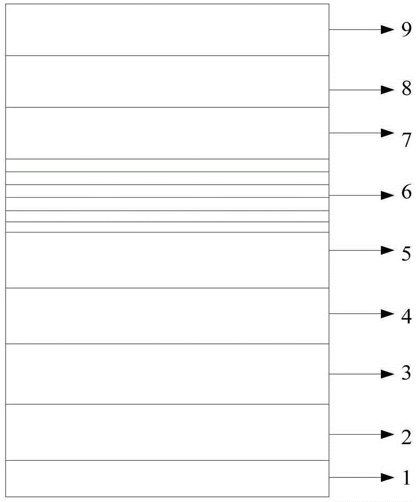
[0048] The present invention uses MOCVD to grow GaN epitaxial layer, adopts high-purity H 2 or high purity N 2 or H 2 and N 2 Mixed gas as carrier gas, high purity NH 3 As the N source, the metal-organic source trimethylgallium (TMGa) is used as the gallium source, trimethylindium (TMIn) is used as the indium source, and the P-type dopant is magnesiumocene (Cp 2 Mg), the substrate is a patterned substrate or a sapphire substrate, and the reaction pressure is between 100mbar and 850mbar. The specific growth method is as follows (for the epitaxial structure, please refer to figure 1 ):

[0049] 1. Treat the substrate: raise the temperature to 1230°C-1280°C, and treat the substrate for 4min-8min;

[0050] 2. Growth of low-temperature buffer layer GaN: reduce the temperature to 520°C-590°C, 2 growing a buffer layer with a thickness of 20nm-35nm on the above substrate under atmosphere;

[0051] 3. Growth of undoped GaN layer: raise the temperature of the reaction chamber to...

Embodiment 2

[0092] The present invention also provides an LED chip obtained by the method for growing the LED epitaxial layer, the substrate of the LED chip sequentially includes:

[0093] Buffer layer: the thickness is 20nm-35nm;

[0094] Undoped GaN layer: the thickness is 2μm-3.5μm;

[0095] N-type GaN layer doped with Si: the thickness is 2μm-3.5μm, and the doping concentration of Si is 8×10 18 atoms / cm 3 ~1.5×10 19 atoms / cm 3 ;

[0096] MQW active layer: including 11-18 overlapping units, each overlapping unit sequentially includes an InGaN well layer with a thickness of 2nm-3.5nm and a GaN barrier layer with a thickness of 8nm-13nm;

[0097] Electron blocking layer: including 4-8 overlapping units, each overlapping unit sequentially includes a P-type AlGaN barrier layer with a thickness of 2.8nm-5nm and an InGaN potential well layer with a thickness of 2.5nm-4nm;

[0098] Mg-doped P-type GaN layer: including a first P-type GaN layer with a thickness of 40nm-80nm, a second P-ty...


PUM

PropertyMeasurementUnit
thicknessaaaaaaaaaa
thicknessaaaaaaaaaa
thicknessaaaaaaaaaa

Abstract

The invention discloses an LED epitaxial layer growth method and an LED chip acquired in the method. To grow a Mg-doped P-type GaN layer, at an N2 atmosphere, a first Mg-doped P-type GaN layer with a thickness of 40nm to 80nm grows on an electron blocking layer; temperature of a reaction chamber rises to 1070 to 1140 DEG C, the reaction chamber has a pressure of 400mbar to 700mbar, and at an H2 and N2 mixed atmosphere, a second Mg-doped P-type GaN layer grows on the first P-type GaN layer; temperature of the reaction chamber rises to 1070 to 1140 DEG C, the reaction chamber has a pressure of 200mbar to 400mbar, and at an H2 and N2 mixed atmosphere, a third Mg-doped P-type GaN layer grows on the second P-type GaN layer. Thus, the antistatic performance and the light emitting efficiency of the LED device are improved.

Description

technical field [0001] The present application relates to the technical field of LED epitaxial design application, in particular, to a method for growing an LED epitaxial layer and an LED chip obtained by the method. Background technique [0002] Light-emitting diode (LED), as a new type of high-efficiency, environmentally friendly and green solid-state lighting source, has the characteristics of small size, light weight, long life, high reliability and low power consumption, and is widely used in outdoor display screens, car lights, traffic lights, etc. Signal lights, landscape lighting, backlight and other fields. [0003] GaN-based materials are mostly grown on sapphire substrates. Due to the large lattice mismatch between GaN-based materials and sapphire substrates, which is about 13.5%, a large number of dislocations and defects will be generated in the epitaxial layer. The defect density up to 1*10 8 -1*10 10 / cm3, and the p-type and n-type electrodes of the GaN-bas...

Claims


Application Information

Patent Timeline
Patent Type & Authority Applications(China)
IPC IPC(8): H01L33/04H01L33/06H01L33/14H01L33/00C30B29/40C30B25/02
CPCC30B25/22C30B29/406H01L33/007H01L33/04H01L33/06H01L33/145
Inventor 刘为刚曾莹
Owner XIANGNENG HUALEI OPTOELECTRONICS
Why Eureka
Try Eureka