

Growth of cubic crystalline phase strucure on silicon substrates and devices comprising the cubic crystalline phase structure
a technology of strucure and crystalline phase, which is applied in the direction of basic electric elements, electrical apparatus, and semiconductor devices, can solve the problems of affecting the efficiency droop effect, the green gap, and the authors' time-consuming and labor-intensive problems, and it took them 8 days to grow such materials
- Summary
- Abstract
- Description
- Claims
- Application Information
AI Technical Summary
Benefits of technology
Problems solved by technology
Method used
Image

Examples
example 1
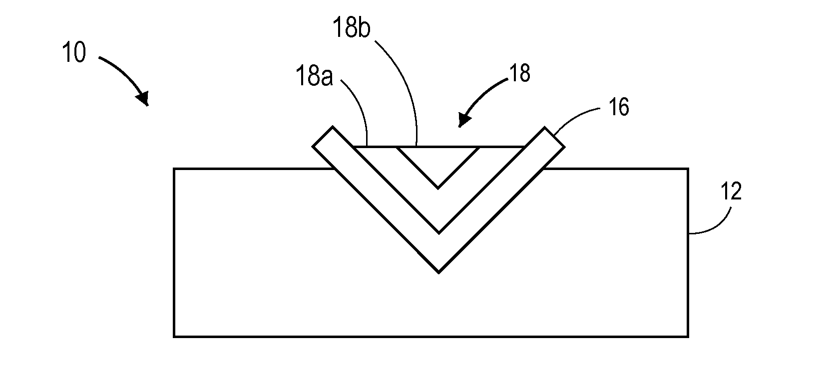
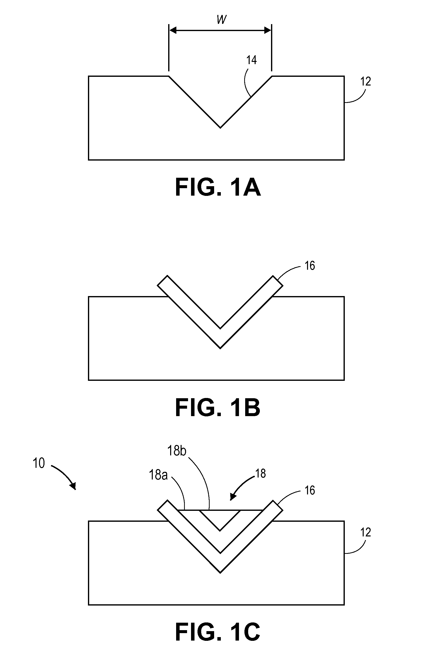
[0107]A line array of v-grooves with a period of 1.8 microns was fabricated into a Si(001) substrate by interferometric lithography with a single longitudinal transverse mode, frequency-tripled, yttrium aluminum garnet laser at a wavelength of 355-nm and anisotropic wet etching based on potassium hydroxide. The lithographic pattern was aligned so that the v-grooves were aligned approximately along the direction of the Si surface. This led to the revealing of {111} sidewalls after KOH etching. As a substrate, boron-doped Si(001) wafers with resistivity of ˜10 ohm-cm were used. An electron beam-deposited Cr film (˜200 nm) was employed as an etch mask. Each groove comprises two (111)-type facets forming a v-shape valley when viewed in cross section. The groove width was kept at ˜0.8 microns and the corresponding depth was then ˜0.6 microns.
[0108]On the v-groove-patterned substrate, a buffer comprising a thin AlN and 450 nm-thick GaN layer was grown first by MOVPE. The thin AlN was emp...
example 2
[0109]On a patterned substrate similar to that of Example 1, an additional 5 stacks of a ˜3 nm-thick InxGa1-xN well with a ˜20 nm-thick GaN spacer, and an ˜8 nm-thick GaN capping layer were consecutively grown on the 450-nm-thick GaN buffer layer. All layer thicknesses, both in Example 1 and Example 2, were calibrated on a sapphire (0001) plane as a reference. The total amount of deposition was sufficient to induce the phase transition to cubic phase by filling up each v-groove. At the same time, the deposition was controlled to avoid any coalescence between the epitaxial layers grown on adjacent grooves. Thus, most of the epitaxial layers grown on individual grooves kept the identical crystal shape even when growing beyond their initial filling of their respective groove.
example 3
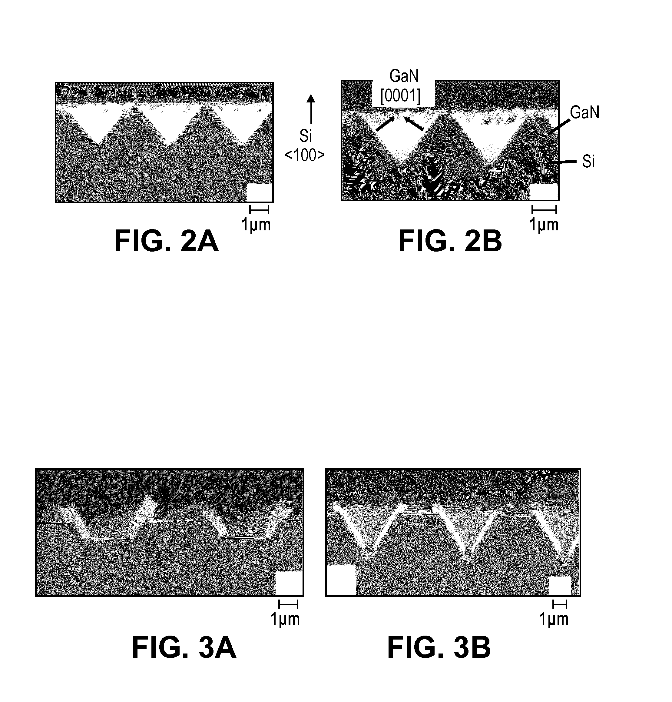
[0110]Examples of different buffer layers are shown in FIG. 2. In FIG. 2B the nucleation layer is about 25% thinner than in FIG. 2A. The resulting growth looks similar in both cases, showing good and selective nucleation normal to {111} planes. In the example of FIG. 2, no growth occurred on the flat top Si (100) surfaces between the v-grooves. The GaN on the sidewalls was smooth and continuous, but the top edges were irregularly shaped. Voids can form where the two wings from adjacent v-grooves join.
PUM
 Abstract
Description
Claims
Application Information