Semiconductor device and a method of manufacturing such a semiconductor device

a semiconductor device and semiconductor technology, applied in the field of semiconductor devices and manufacturing methods, can solve the problems of increasing the cost of semiconductor devices, so as to improve the reliability, improve the performance, and reduce the thermal problems of self-heating

Inactive Publication Date: 2007-11-01
INFINEON TECH AG
View PDF10 Cites 25 Cited by
  • Summary
  • Abstract
  • Description
  • Claims
  • Application Information

AI Technical Summary

Benefits of technology

[0005] The invention provides a CMOS device which has an improved performance over conventional devices. In preferred embodiments, the invention provides a CMOS device in which thermal problems, namely self-heating, are reduced as compared with conventional devices. The invention also provides a CMOS device that has an improved reliability as compared to conventional devices and one which can be produced with a low fabrication time and cost.
[0007] It will be appreciated that in the invention dissimilar semiconductor materials are used to form the channel regions of the first and second field effect transistors so that high electron and hole mobility can be achieved.
[0009] Preferably also, the first, n-type conductivity semiconductor material used for the first channel also comprises silicon and the second p-type conductivity semiconductor material used for the second channel comprises a SiGe alloy. This keeps the benefits of the existing electron mobility of Si material and the higher hole mobility of Ge / SiGe material in order that a more balanced CMOS chip can be designed with improved speed performance.
[0010] Advantageously, however, on a silicon substrate the first, n-type conductivity semiconductor material used for the first channel comprises a different material to that of the substrate. In a preferred embodiment, gallium arsenide (GaAs) is used as the first, n-type conductivity semiconductor material for the first channel and silicon-germanium (SiGe) is used as the second p-type conductivity semiconductor material for the second channel. This enables an even faster chip to be designed with further enhanced speed performance. Compared to conventional Si (silicon: μn=1350 cm2 / V-s) technology, a GaAs (Gallium Arsenide: μn=8500 cm2 / V-s) material system exhibits superior transport properties, namely a five times higher electron mobility and higher low field electron velocity. Similarly, the electron and hole mobility values of Ge (μn=3900 cm2 / V-s, μh=1900 cm2 / V-s) and Si0.75Ge0.25 (μn=2100 cm2 / V-s, μh=812 cm2 / V-s) are superior to that of Si.
[0012] There is, however, a heteroepitaxy growth problem associated with the direct growth of a GaAs layer to form the first, n-type conductivity semiconductor material for the first channel on a Si or GaP substrate as there is a large lattice mismatch. The lattice constant of GaAs is 4.6532 Å as compared to that for silicon of 5.431 Å. Preferably, therefore, at least one but advantageously a plurality of intermediate layers each in the form of a superlattice stack is provided between the Si basal substrate layer and the GaAs layer forming the first channel to absorb the lattice mismatching between GaAs and Si. The growth of GaAs on a GaP / Si substrate can therefore be achieved.

Problems solved by technology
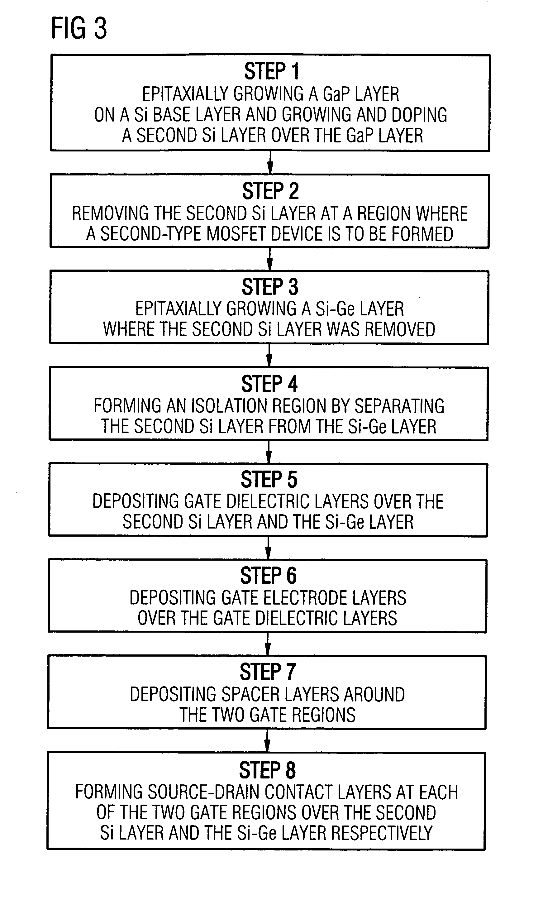
Improvement of performance in conventional silicon MOS and CMOS technologies through reduction of feature size, is becoming extremely difficult, if not impossible.
Additionally, the electrical properties (i.e., material transport properties such as carrier mobility) of silicon itself provide another source of performance limitation in terms of propagation delay.
It should be noted here that conventional bulk silicon and SOI based CMOS transistors, which comprise n- and p-channel MOS transistors on the same substrate (i.e. silicon) suffer from imbalance owing to different electron and hole mobility values.
Also, this imbalance of electron and hole-mobility in CMOS devices is further exacerbated in devices with strained silicon channels, since the strained silicon channel (i.e. process induced strain in Si and Si channel on relaxed SiGe type) does not enhance the hole mobility in p-MOS transistors as much as it does the electron mobility in n-MOS transistors.
Another common problem associated with all SOI type CMOS devices is the self heating effect.
Devices operating at high drain voltage and current suffer from the reduction of carrier mobility and saturation velocity, resulting in reduction in the drain current and transconductance.
Other severe problems such as increased electromigration and enhanced impact ionization because of increased device heating, affect the reliability of the devices.
This problem is basically associated with difference in the thermal conductivities of silicon (Si), silicon-germanium alloys (SiGe) and silicon dioxide (Sio2) for all the SOI type devices discussed earlier.

Method used


Image

  • Semiconductor device and a method of manufacturing such a semiconductor device
  • Semiconductor device and a method of manufacturing such a semiconductor device
  • Semiconductor device and a method of manufacturing such a semiconductor device

Examples


Embodiment Construction

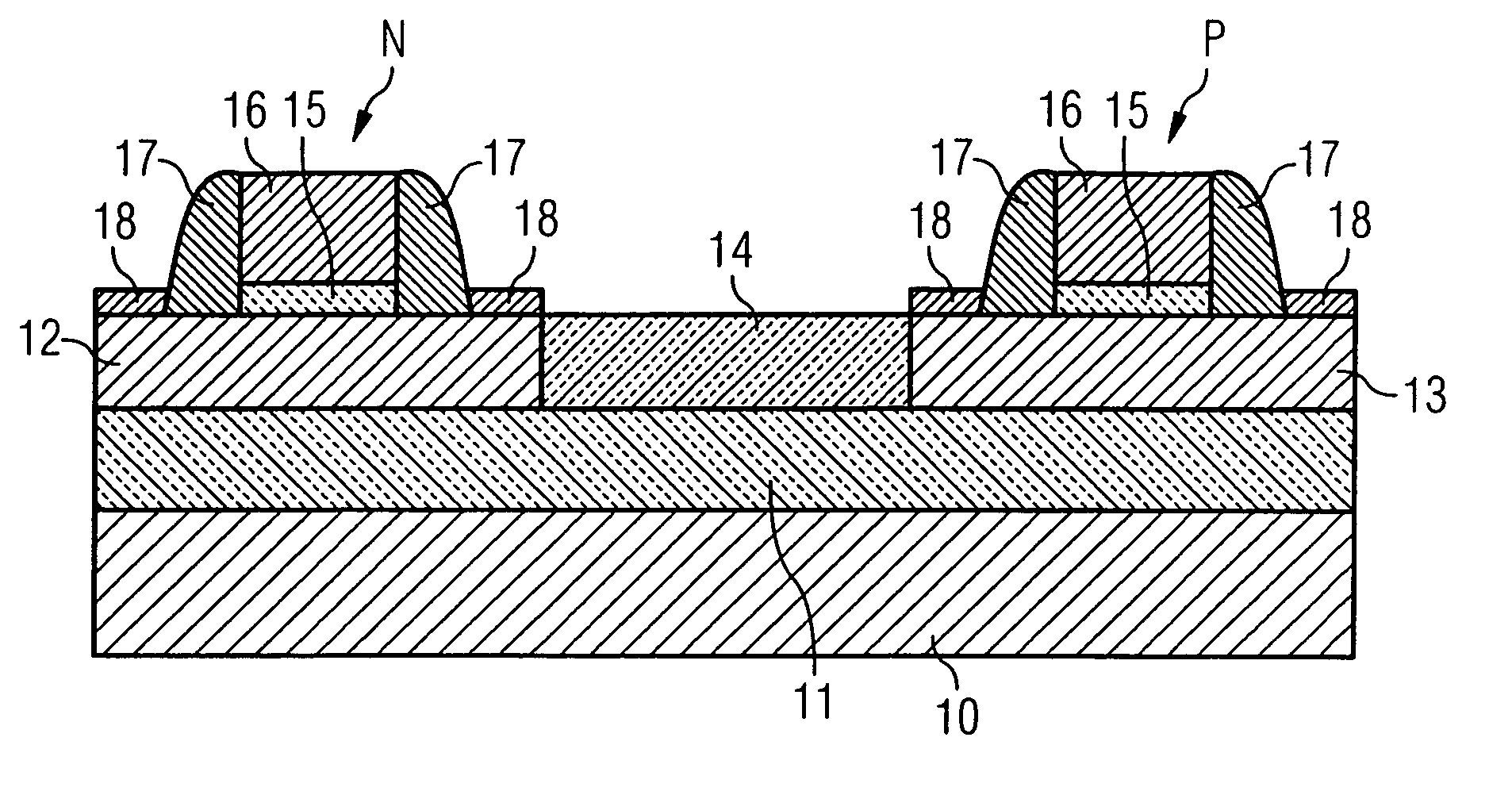
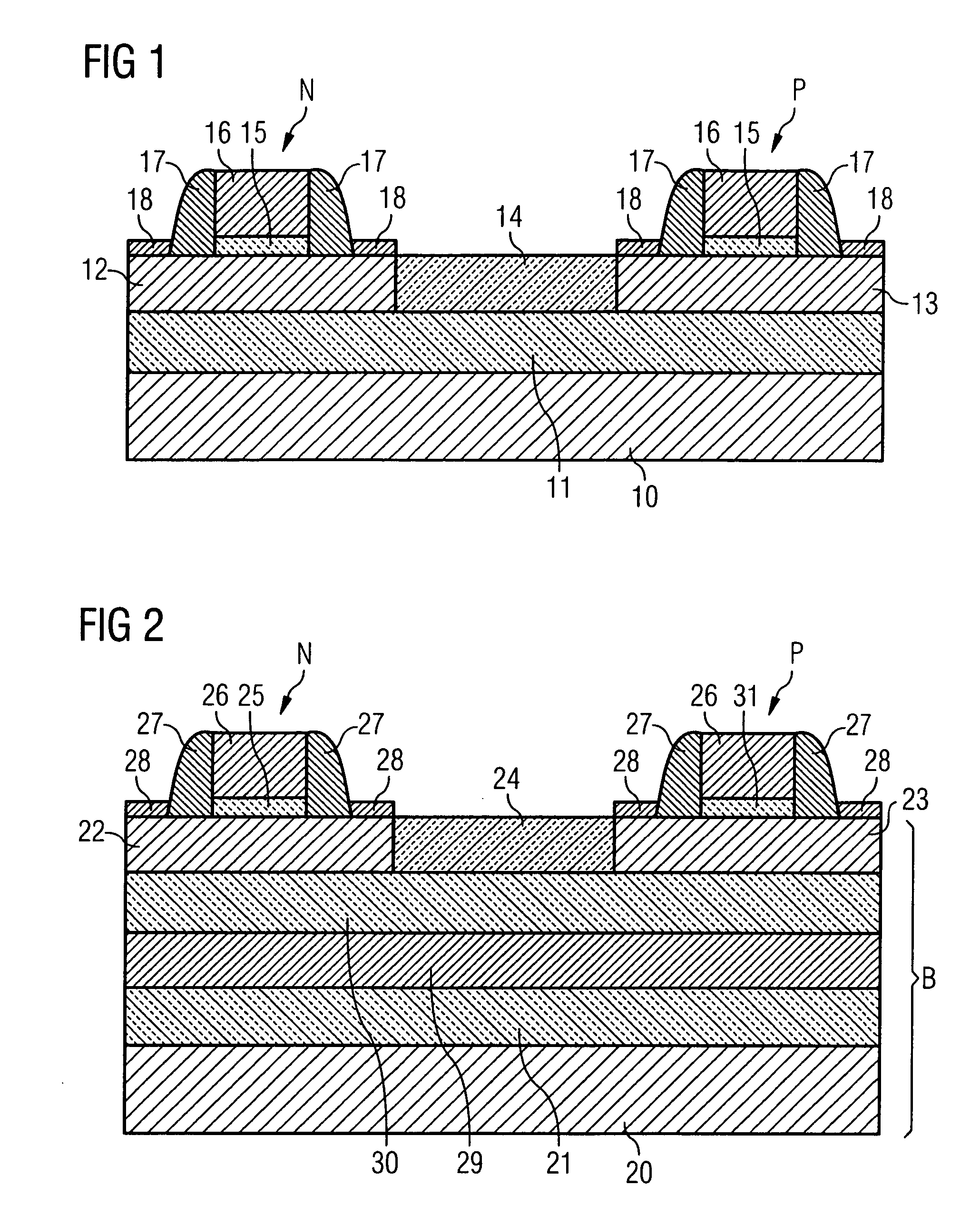
[0022] In both of the semiconductor devices shown in FIGS. 1 and 2, multiple semiconductor materials are integrated to form the device on a Si substrate 10 and 20 respectively. It should be noted that both FIG. 1 and FIG. 2 are diagrammatic and are not drawn to scale, the dimensions of the thicknesses of the various layers of semiconductor materials being exaggerated for greater clarity. Corresponding parts in both figures are given the same hatching and generally have the same references numerals but separated by ten, for example the Si substrate in FIG. 1 has the reference numeral 10 whereas in FIG. 2 the Si substrate has the reference numeral 20.

[0023] In both FIG. 1 and FIG. 2, the semiconductor device comprises a CMOS device wherein both an n-MOSFET device N and a p=MOSFET device P are formed on the same Si substrate 10, 20.

[0024] In the first embodiment shown in FIG. 1, the substrate also comprises a layer 11 of GaP provided over a base Si layer 10 to provide insulation and ...


PUM


Abstract

A semiconductor device, specifically a Complementary Metal Oxide Semiconductor (CMOS) device, has a substrate on which are formed first and second field effect transistors. Each of the field effect transistors comprises a source-drain region, a channel of either an n-type or a p-type conductivity semiconductor material formed on the substrate, a first gate region, and a first dielectric region that separates the first channel from the first gate region. However, dissimilar semiconductor materials are used to form the channel regions of the first and second field effect transistors so that high electron and hole mobility can be achieved.

Description

TECHNICAL FIELD OF THE INVENTION [0001] The invention relates to a semiconductor device and method of manufacturing a semiconductor device. BACKGROUND OF THE INVENTION [0002] Mainstream semiconductor device production currently tends to center on conventional silicon and silicon-on-insulator (SOI) based Metal Oxide Semiconductor (MOS) and CMOS technologies. The main thrust of research is based around reduction in device feature size to nanometer scale that thereby provides improvements in the device performance. As the performance of a CMOS chip is generally measured by its integration density, switching speed and power dissipation, the transistor channel length and parasitic resistive-capacitive (RC) constant are the two major contributors that finally limit the circuit speed. The transistor switching delay (i.e. propagation delay) of a typical CMOS device, is a function of the device load capacitance, the drain voltage, and the saturation currents for both the n- and p-channel dev...

Claims


Application Information

Patent Timeline
Patent Type & Authority Applications(United States)
IPC IPC(8): H01L29/78H01L21/8238
CPCH01L21/28255H01L21/28264H01L29/78H01L21/8258H01L29/517H01L21/823807
Inventor MUHAMMAD, NAWAZ
Owner INFINEON TECH AG
Why Eureka
Try Eureka