Chip encapsulation substrate assembly and chip encapsulation construct

A chip packaging and substrate technology, applied in electrical components, electrical solid devices, circuits, etc., can solve the problems of pin and chip bump peeling, insufficient bonding strength between pins and chip bumps, and decreased manufacturing yield. Improve package yield and reliability, prevent pin stripping, and increase contact area

Inactive Publication Date: 2009-04-22
CHIPMOS TECH INC
View PDF0 Cites 4 Cited by
  • Summary
  • Abstract
  • Description
  • Claims
  • Application Information

AI Technical Summary

Problems solved by technology

[0005] However, the joint strength between the lead and the chip bump is likely to be insufficient, so that the phenomenon of peeling between the lead and the chip bump occurs, which leads to a tape carrier package (TCP) structure or a film-on-chip package ( COF) structure manufacturing yield decline

Method used


Image

  • Chip encapsulation substrate assembly and chip encapsulation construct
  • Chip encapsulation substrate assembly and chip encapsulation construct
  • Chip encapsulation substrate assembly and chip encapsulation construct

Examples


Embodiment Construction

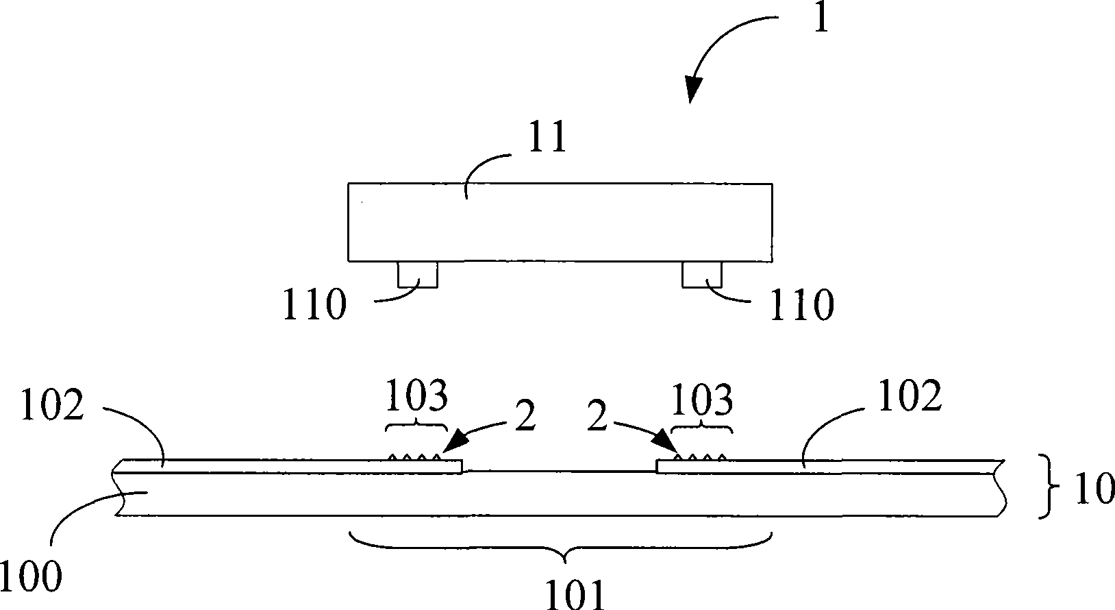
[0028] The first embodiment of the present invention is a chip packaging structure 1, and its cross-sectional view is as follows figure 1 shown. The chip packaging structure 1 includes a chip packaging substrate assembly 10 and a chip 11 . The chip package substrate assembly 10 includes a flexible dielectric layer 100 and a plurality of pins 102 . In practical applications, the chip package structure 1 can be a tape carrier package (TapeCarrier Package, TCP) or a chip-on-film package (Chip-On-Film, COF).

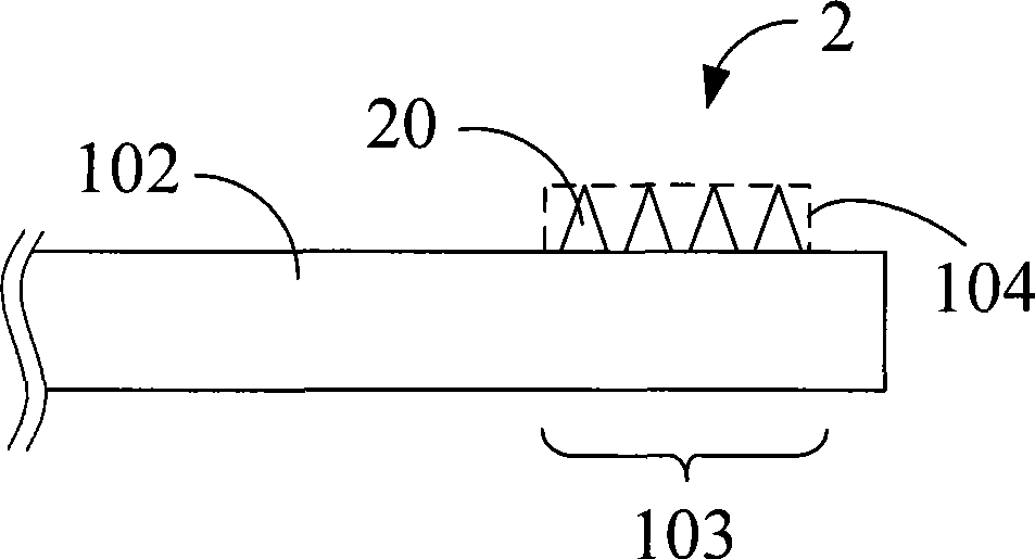
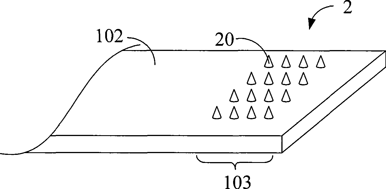
[0029] A chip bonding area 101 is defined on the flexible dielectric layer 100 . The flexible dielectric layer 100 can be an organic dielectric film layer made of materials such as polyimide (PI) or polyethylene terephthalate (PET). With the organic dielectric film layer, the pins 102 can be fixed on the chip packaging substrate assembly 10 , and the pins 102 can be electrically isolated.

[0030] In this embodiment, the pin 102 is made of a material with high conductivi...


PUM


Abstract

The invention relates to a chip packaging substrate assembly for a chip packaging structure and the chip packaging structure containing the chip packaging substrate assembly, and the chip packaging substrate assembly comprises a flexible dielectric layer and a plurality of pins and chips. A chip bonding area is defined on the flexible dielectric layer; a plurality of pins are formed on the flexible dielectric layer, the inner ends of the various pins are further extended into the chip bonding area, acute raised structures are formed on the various inner ends; each chip is provided with a plurality of bumps, when in para-position combination of the chips and the chip bonding area, the acute raised structures can be correspondingly embedded in a plurality of bumps.

Description

technical field [0001] The invention relates to a chip packaging substrate assembly for chip packaging structure and a chip packaging structure including the chip packaging substrate assembly. In more detail, it relates to a chip package substrate assembly including a chip package structure including a plurality of bumps and a plurality of pins, and a chip package structure including the chip package substrate assembly. Background technique [0002] In recent years, with the continuous maturity and development of semiconductor process technology, various high-efficiency electronic products have been continuously introduced, and the integration of integrated circuit (Integrated Circuit, IC) chips has also been continuously improved. Integrated circuit chip packaging types can be roughly divided into Wire Bonding Package (Wire Bonding Package), Tape Automatic Bonding Package (Tape Automatic Bonding, TAB) and Flip Chip Package (Flip Chip Package), and each package type has It ...

Claims


Application Information

Patent Timeline
Patent Type & Authority Applications(China)
IPC IPC(8): H01L23/498H01L23/48
CPCH01L2224/16225H01L2224/81385
Inventor 陈煜仁毛苡馨
Owner CHIPMOS TECH INC
Why Eureka
Try Eureka