
Semiconductor element

A semiconductor and power semiconductor technology, applied in the direction of semiconductor devices, electrical components, transistors, etc., can solve the problems of reducing the temperature of components, speeding up the switching rate of transistor switching, etc., to achieve the effect of increasing the switching rate, reducing temperature, and reducing noise interference

Inactive Publication Date: 2010-06-09
泓广科技有限公司
View PDF4 Cites 0 Cited by
  • Summary
  • Abstract
  • Description
  • Claims
  • Application Information

AI Technical Summary

Problems solved by technology

[0005] The main purpose of the present invention is to provide a kind of CMOS semiconductor element, to overcome the shortcoming of the arc-shaped corner of the existing transistor grid, to achieve mutual interference between the signals, so as to make the driven current smooth and stable, to speed up The switching rate of the transistor switch can reduce the temperature of the component during operation and increase the overall reliability of the component

Method used


Image

  • Semiconductor element
  • Semiconductor element
  • Semiconductor element

Examples


Embodiment Construction

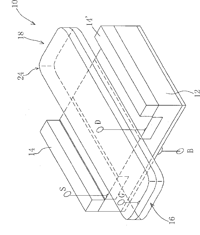
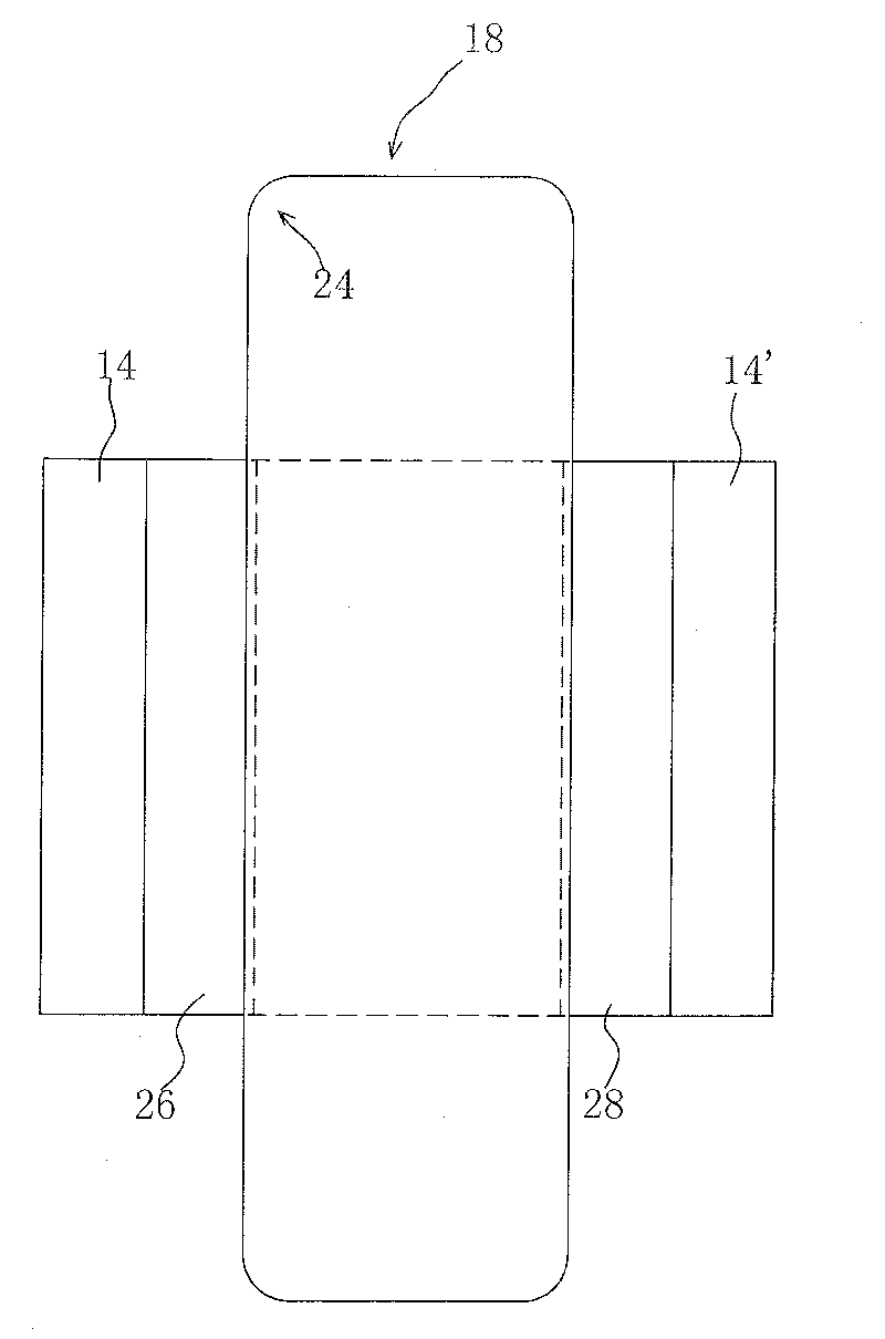
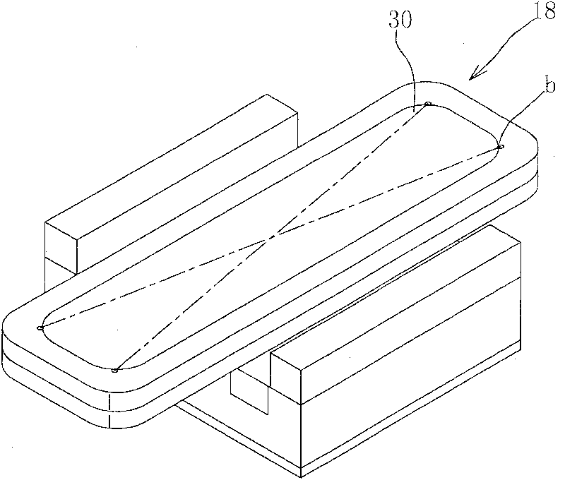
[0022] In view of the fact that the gate structure of the metal oxide field effect transistor of the conventional semiconductor element forms a round structure at the corner, the current driving direction will be disordered, the ohmic heat will increase, the life of the element will be reduced, and the reliability will be reduced. The corners of the shape gate structure are parabolic-shaped brand-new semiconductor elements, and the apexes of the corners are rounded to use the optical properties of the parabola, rectify the driving direction of the current, reduce mutual interference, and increase the switching rate of the semiconductor element.

[0023] Please also refer to figure 1 and figure 2 , which is a three-dimensional schematic view and a top view of the CMOS semiconductor device of the present invention. As shown in the figure, the transistor structure 10 includes a P-type semiconductor substrate (or N-well, N well) 12; two isolation structures 14, 14' each located ...


PUM


Abstract

The invention provides a semiconductor element. The semiconductor element comprises at least one grate structure with the corner being a parabolic shape, and the center of the corner is at the vertexof the parabola so as to realize noninterference among signals by the optical focusing property of the parabola and to cause the driven current to be smooth and orderly, thus increasing the switchingrate of a transistor switch, lowering temperature of the semiconductor element temperature during operation, and enhancing the overall reliability of the semiconductor element.

Description

technical field [0001] The invention relates to a semiconductor element, in particular to a transistor element and a power semiconductor element with an improved gate structure. Background technique [0002] Semiconductor elements are composed and driven by many metal oxide field effect transistors (MOSFETs). In the CMOS process, the gate shapes of NMOS and PMOS are generally connected to long strips due to process and functional requirements, and the power The shape of the gate structure of the semiconductor element can basically be any shape, such as a triangle, a quadrangle, an octagon, and the like. [0003] When starting a semiconductor device, once many MOSs are driven at the same time, the current contributed by all units will add up to form the designed power or current. However, in order to avoid the tip discharge of the gate structure of the traditional metal oxide field effect transistor (MOSFET), the corners will form an arc shape, but such arc-shaped corners wi...

Claims


Application Information

Patent Timeline
Patent Type & Authority Patents(China)
IPC IPC(8): H01L27/092H01L29/78H01L29/423H01L29/06
Inventor 杨信佳郭志盛
Owner 泓广科技有限公司
Learn More