Supercharge Your Innovation With Domain-Expert AI Agents!

Filtering device and method used for dual frequency band sensing circuit

A sensing circuit and filtering device technology, applied in electrical components, transmission systems, diversity/multi-antenna systems, etc., can solve the problems of large module loss, large attenuation, and insufficient flexibility of RF filters, etc., to reduce loss and eliminate interference effect

Inactive Publication Date: 2009-04-29
AZUREWAVE TEHNOLOGIES INC
View PDF1 Cites 2 Cited by
  • Summary
  • Abstract
  • Description
  • Claims
  • Application Information

AI Technical Summary

Problems solved by technology

However, the higher the order of the filter, the greater the loss in the module. That is, although the required energy requirement can be achieved, the greater the circuit area and the longer the path of the radio frequency, the greater the attenuation
[0003] Moreover, if it is applied to high-frequency communication modules in the prior art, such as wireless local area networks (such as WLAN, WiMax, etc.), mobile communication technologies (such as GSM, 3G, etc.), if it needs to coexist with different frequency band subsystems in design, For example, the coexistence design of different frequency bands (1.8GHz, 5GHz, etc.) usually needs to add a filter with an additional transmission zero to avoid interference. However, adding a transmission zero will increase the circuit design in the module and increase the bandwidth. In-band loss
[0004] In addition to the use of filters in the above-mentioned frequency bands, or the application between different frequency bands, in fact, even if the above-mentioned different frequency band subsystems operate at the same time, the degree of interference may not have a significant impact on the entire interfered system; and these different frequency bands The subsystems do not necessarily act at the same time, but alternately operate as needed. Therefore, the use of general RF filters is not flexible enough

Method used


Image

  • Filtering device and method used for dual frequency band sensing circuit
  • Filtering device and method used for dual frequency band sensing circuit
  • Filtering device and method used for dual frequency band sensing circuit

Examples


Embodiment Construction

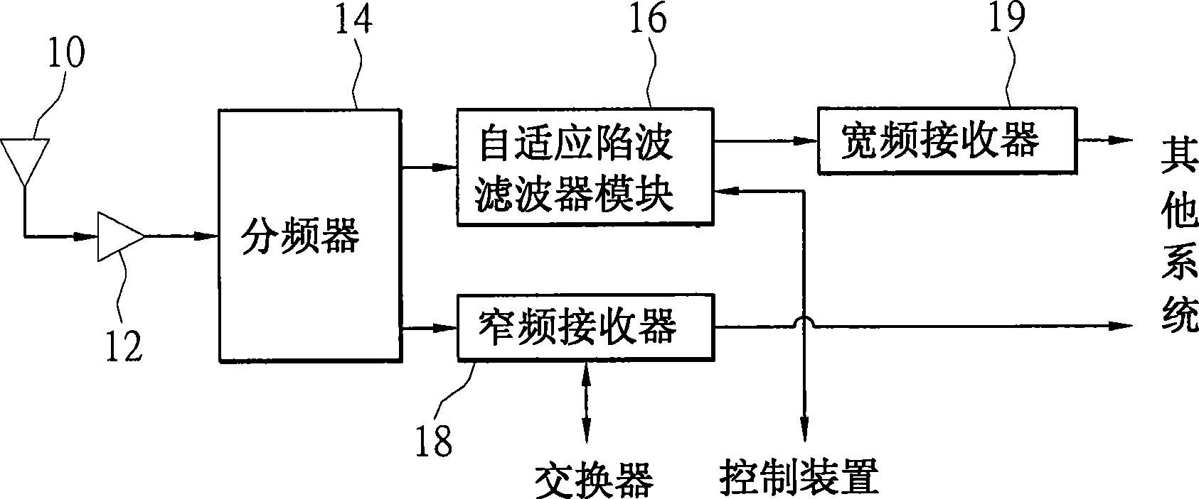
[0036] Band rejection filter (Notch Filter) is a kind of filter, and the band rejection filter is to filter out the signal of a specific frequency band. The present invention provides a filter device and method used in a dual-band sensing circuit in the field of wireless communication. When an adaptive notch filter is set on the path of a radio frequency signal (RF signal), it can Judging the current interference intensity to enable high-frequency or low-frequency band-rejection filters, you can simply control the bandwidth of the filter to filter a specific frequency band, reduce the loss in the band, and reflect the desired signal.

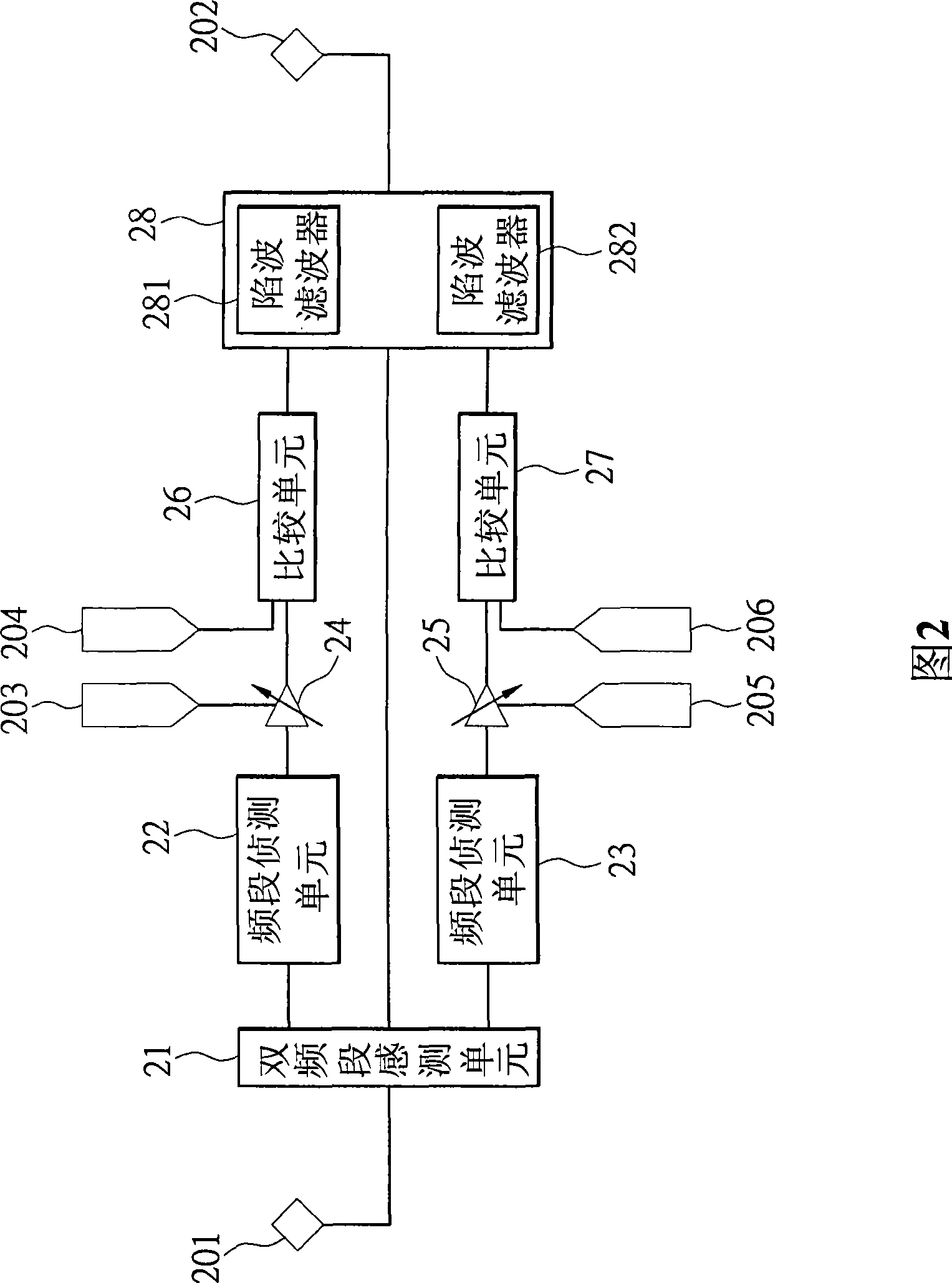
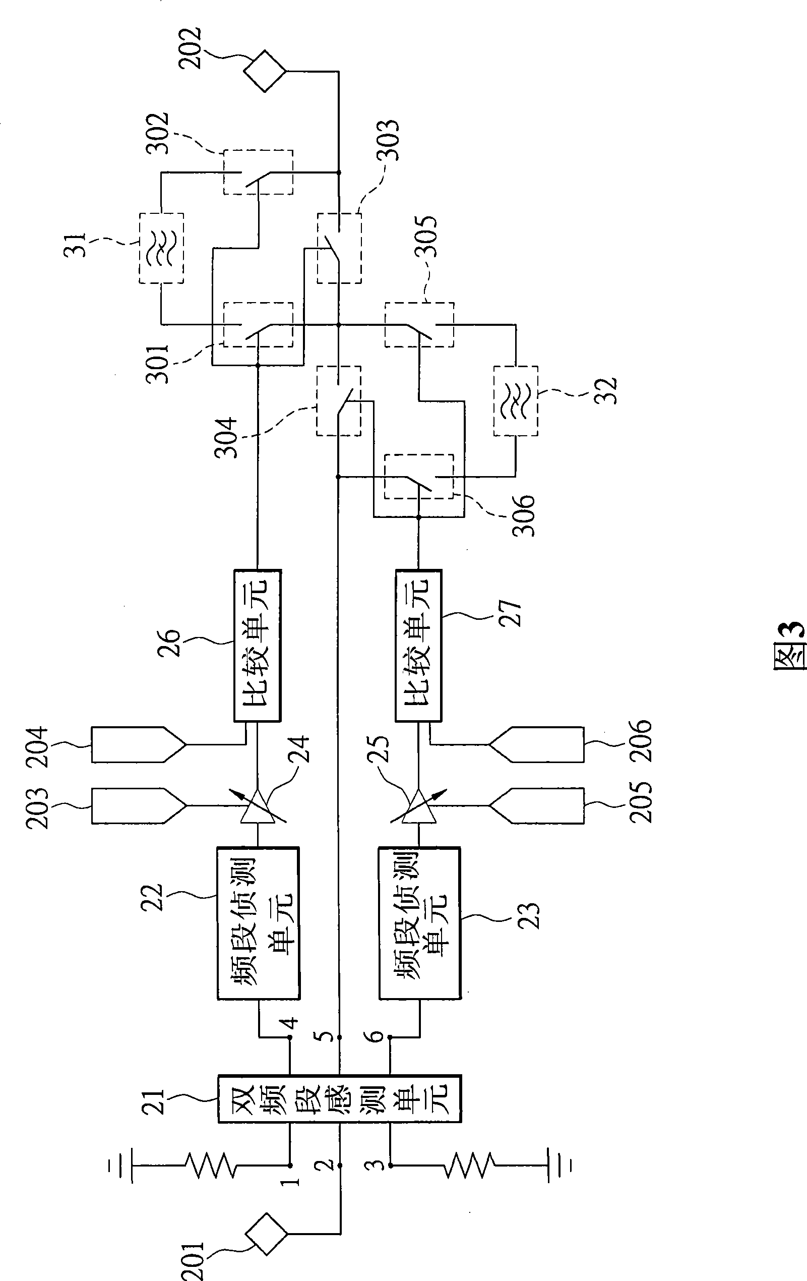
[0037] Please refer to FIG. 2 , which shows an embodiment of the filter device used in the dual-band sensing circuit of the present invention. The filter device is connected to an external signal source through a connection port 201. A preferred embodiment is to connect different frequency band subsystems coexisting. communication module. In th...


PUM


Abstract

The present invention relates to a filtering device for dual band sensing circuit and a method thereof. The present invention is characterized in that a dual band sensing unit provided on a filtering device is used for receiving signals from a different frequency band subsystem and performing frequency division, then, one or more frequency band detecting units are used for detecting energy of signals at the high frequency band and the low frequency band and converting the energy into voltage, and users can adjust the gain of a tunable gain amplifier through an external part, perform a comparison operation by using a comparison unit, and control the switch time of a radio frequency switch unit with the help of generated signals, therefore, an adaptive notch filter effect is achieved, the notch filter with a high frequency or a low frequency is started by judging the current interference intensity, thus, in-band wastage is reduced.

Description

technical field [0001] The present invention relates to a filter device and method used in a dual-band sensing circuit, in particular to controlling the signal gain externally to determine the opening timing of a band rejection filter to effectively suppress interference. Background technique [0002] Generally, when designing a high-frequency communication module, the operating frequency band will be designed according to the requirements. At this time, a radio frequency filter (RF filter) is usually used to filter the required frequency band. If the frequency band or energy to be filtered is higher, the order of the filter required is higher. Different designs have different order requirements. However, the higher the order of the filter, the greater the loss in the module. That is, although the required energy requirement can be achieved, the greater the circuit area and the longer the radio frequency path, the greater the attenuation. [0003] Moreover, if it is applied...

Claims


Application Information

Patent Timeline
Patent Type & Authority Applications(China)
IPC IPC(8): H04B1/10H04B7/02
Inventor 黄忠谔简煌展
Owner AZUREWAVE TEHNOLOGIES INC
Features
  • R&D
  • Intellectual Property
  • Life Sciences
  • Materials
  • Tech Scout
  • Unparalleled Data Quality
  • Higher Quality Content
  • 60% Fewer Hallucinations
Learn More