Photovoltaic device with nanostructured layers

A photovoltaic device and nanostructure technology, which is applied to the surface coating liquid device, coating, special surface, etc., can solve the problems of difficult processing temperature, inability to obtain, poor efficiency, etc.

Inactive Publication Date: 2009-04-29
SOLEXANT CORP (US)
View PDF0 Cites 2 Cited by
  • Summary
  • Abstract
  • Description
  • Claims
  • Application Information

AI Technical Summary

Problems solved by technology

The two main problems with CIGS solar cells are: (1) there is no clear route to higher efficiencies and (2) the high processing temperatures make it difficult to use high speed rolls for roll processing and thus cannot obtain materials that can be made from amorphous silicon. Significantly lowe

Method used


Image

  • Photovoltaic device with nanostructured layers
  • Photovoltaic device with nanostructured layers
  • Photovoltaic device with nanostructured layers

Examples


Embodiment Construction

[0066] Embodiments of the invention relate generally to the field of photovoltaic or solar cells. More particularly the present invention provides photovoltaic devices having IR and / or UV absorbing nanostructured layers. The terms photovoltaic device and solar cell are used interchangeably throughout the description.

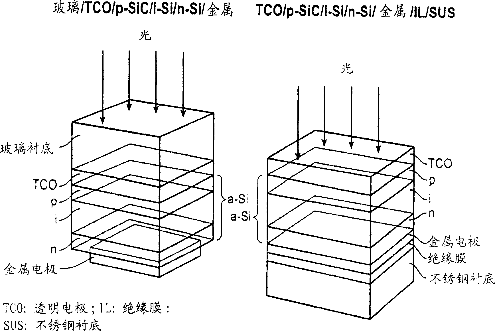
[0067] The invention further relates to cost-effectively increasing the efficiency of solar cells by integrating IR photon absorption or harvesting and / or UV photon absorption or harvesting nanostructured materials. In some embodiments, nanostructured materials are associated with crystalline silicon (monocrystalline or polycrystalline) solar cells and thin film (amorphous silicon, microcrystalline silicon, CdTe, CIGS, and III-V materials) solar energy that absorb primarily in the visible region. One or more integrations in the battery. In some embodiments, the nanostructured material includes one or more nanoparticles integrated with a first layer of material...


PUM


Abstract

Photovoltaic devices or solar cells are provided. More particularly, the present invention provides photovoltaic devices having IR and/or UV absorbing nanostructured layers that increase efficiency of solar cells. In some embodiments the nanostructured materials are integrated with one or more of: crystalline silicon (single crystal or polycrystalline) solar cells and thin film (amorphous silicon, macrocrystalline silicon, CdTe, CIGS and III-V materials) solar cells whose absorption is primarily in the visible region. In some embodiments the nanoparticle materials are comprised of quantum dots, rods or multipods of various sizes.

Description

technical field [0001] In general, the present invention relates to the field of photovoltaics or solar cells. The invention more particularly relates to photovoltaic devices having nanostructured layers. Background technique [0002] Rising oil prices have increased the importance of developing cost-effective renewable energy. Efforts are underway worldwide to develop cost-effective solar cells to harvest solar energy. Current solar technologies can be broadly classified into crystalline silicon and thin film technologies. More than 90 percent of solar cells are made of silicon—monocrystalline, polycrystalline or amorphous. [0003] Crystalline silicon (c-Si) has historically been used as the light-absorbing semiconductor in most solar cells, although it is a relatively poor light-absorbing material and requires comparable material thicknesses (hundreds of microns). However, it has proven convenient since it produces stable solar cells with good efficiencies (12-20%, ha...

Claims


Application Information

Patent Timeline
IPC IPC(8): B05D5/12
Inventor 达莫德·雷迪
Owner SOLEXANT CORP (US)
Why Eureka
Try Eureka