Driving circuit for semiconductor element

A driving circuit and semiconductor technology, applied in the direction of electrical components, electronic switches, output power conversion devices, etc., can solve problems such as false detection, gate voltage exceeding, etc.

Inactive Publication Date: 2009-04-29
MITSUBISHI ELECTRIC CORP
View PDF1 Cites 11 Cited by
  • Summary
  • Abstract
  • Description
  • Claims
  • Application Information

AI Technical Summary

Problems solved by technology

[0004] However, in the drive circuit for power semiconductor elements disclosed in Patent Document 1, when the next turn-on pulse arrives before the gate voltage of the power semiconductor element (IGBT) drops completely, the gate voltage exceeds the reference voltage. value, there is a problem of false detection of anomalies

Method used


Image

  • Driving circuit for semiconductor element
  • Driving circuit for semiconductor element
  • Driving circuit for semiconductor element

Examples


Embodiment approach 1

[0040] Embodiment 1 of the present invention will be described below based on the drawings.

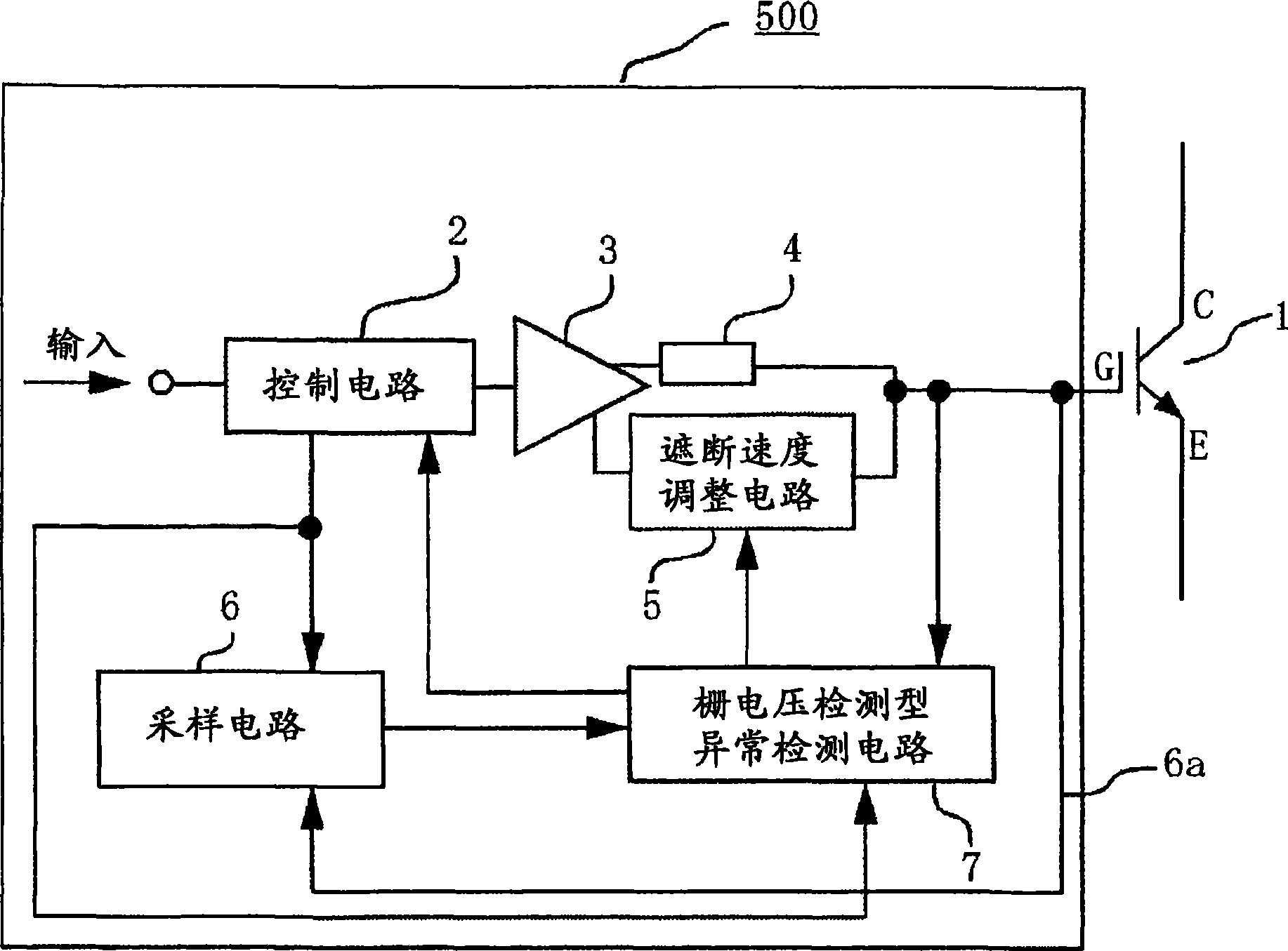
[0041] figure 1 It is a schematic configuration diagram of the driving circuit 500 for the semiconductor element of the first embodiment.

[0042] exist figure 1 Among them, the semiconductor element 1 is, for example, a power semiconductor element IGBT (Insulated Gate Bipolar Transistor). However, the semiconductor element 1 is not limited to an IGBT, and may be a voltage-driven semiconductor element such as a MOSFET, as long as it is necessary for abnormality detection.

[0043] The control circuit 2 outputs a gate command to turn on the IGBT 1 to the buffer 3 when an external turn-on command is input, and outputs a gate command to turn off the IGBT 1 to the buffer 3 when an external turn-off command is input. Buffer 3 drives IGBT 1 according to a gate command output from drive circuit 2 , and is connected to gate resistor 4 and shutoff speed adjustment circuit 5 . The shutoff s...

Embodiment approach 2

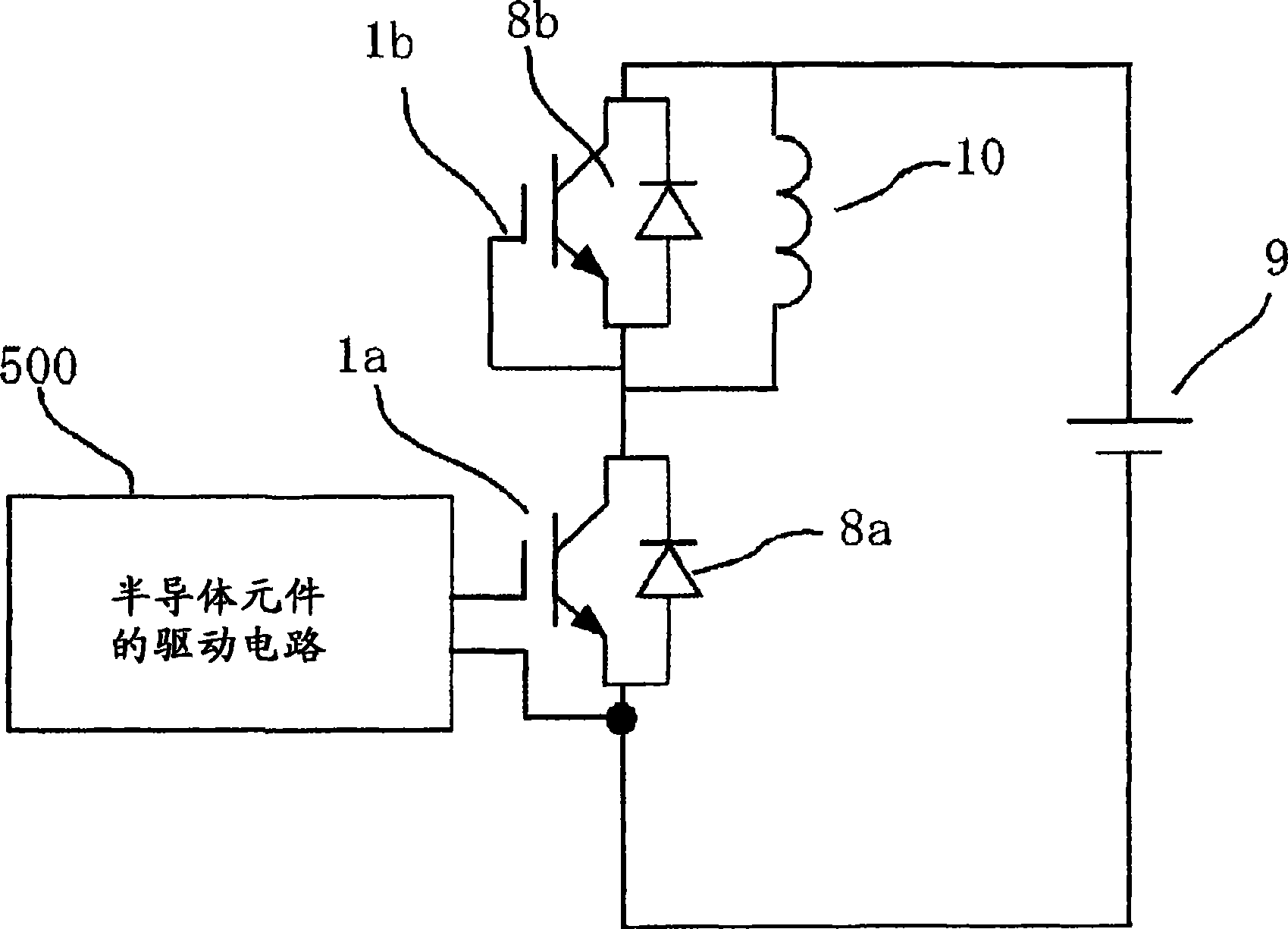
[0069] Embodiment 2 of the present invention will be described below based on a drive circuit 500 a shown in FIG. 17 .

[0070] In Embodiment 1, the gate voltage Vg of the IGBT 1 is directly detected, and the gate voltage detection period T2 and the reference voltage Vgr are changed. In Embodiment 2, as shown in FIG. 17 , in Embodiment 1 figure 1 A gate voltage estimating circuit 8 is added to the configuration of the drive circuit 500 shown. The gate voltage estimating circuit 8 estimates a gate voltage using a control signal from the control circuit 2 and outputs it to the sampling circuit 6 and the gate voltage detection type abnormality detection circuit 7 , and operates in the same manner as in the first embodiment.

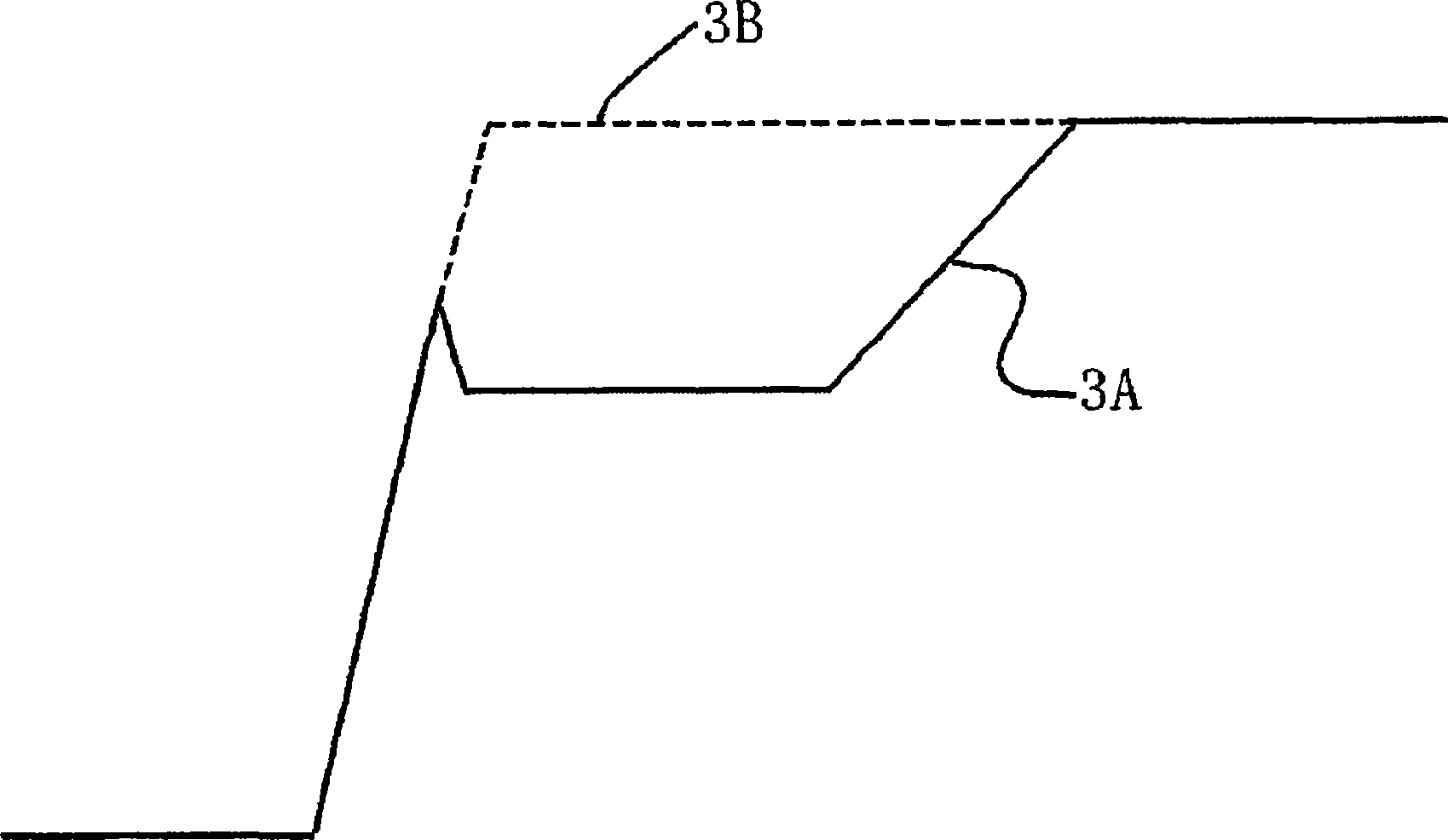
[0071] Figure 18 A control signal, a gate voltage, and an estimated value of the gate voltage are shown. With the delay circuit 79 shown in FIG. 17, the time from when the control signal sends out the turn-on pulse to when the gate voltage Vg rises is de...

Embodiment approach 3

[0075] Next, Embodiment 3 of the present invention will be described.

[0076] FIG. 19 is a schematic configuration diagram of a driving circuit 500b for a power semiconductor element according to the third embodiment. In FIG. 19 , the same reference numerals as those in FIG. 10 of Embodiment 1 denote the same or corresponding parts, and description thereof will be omitted. In addition, 4c is a turn-on gate resistance, 4d is a turn-off gate resistance, 7a is a gate current detection type abnormality detection circuit, and 87 is a gate current comparison circuit. The gate current detection type abnormality detection circuit 7a uses the differential amplifier 85 to detect the voltage across the turn-on gate resistor 4c, and detects the abnormality of the IGBT 1 by detecting that the gate current Ig within the detection period set by the sampling circuit 6 is smaller than the threshold value. The gate current threshold value Igr of the gate current detection type abnormality det...


PUM


Abstract

A driving circuit for a semiconductor element eliminates false detection of an abnormality of a semiconductor element (1) when a gate-on command is inputted in a status where the gate voltage of the semiconductor element (1) is not sufficiently lowered. A control quantity (gate voltage) of the semiconductor element (1) is permitted to be detected only during a period which corresponds to a control quantity (Qon) of the semiconductor element (1) when an on-signal is inputted to a control circuit (2), a detected control quantity (Qt) detected during the period is compared with a control comparison quantity (Qs) set by corresponding to the control quantity (Qon) to output an abnormal signal, and the semiconductor element (1) is shut off at a speed lower than a normal shutoff speed.

Description

technical field [0001] The present invention relates to a drive circuit for a semiconductor element that detects an abnormality occurring in the semiconductor element, and more particularly to a drive circuit for a power semiconductor element. Background technique [0002] As a drive circuit of a conventional power semiconductor element (IGBT), there has been disclosed a technique in which a sampling circuit detects the gate voltage during the detection process of allowing the gate voltage, and if the gate voltage exceeds a reference value, it recognizes that the IGBT is An abnormality occurs (for example, refer to Patent Document 1). [0003] [Patent Document 1] Japanese Unexamined Patent Publication No. 2004-064930 (lines 31-37 of page 7, figure 1 ) [0004] However, in the drive circuit for power semiconductor elements disclosed in Patent Document 1, when the next turn-on pulse arrives before the gate voltage of the power semiconductor element (IGBT) drops completely, t...

Claims


Application Information

Patent Timeline
Patent Type & Authority Applications(China)
IPC IPC(8): H02M1/08H02M1/00H03K17/08
CPCH03K17/08128H03K17/18H03K17/168
Inventor 中武浩石桥诚司井手之上慎介大井健史木之内伸一堀口刚司
Owner MITSUBISHI ELECTRIC CORP
Why Eureka
Try Eureka