Method for manufacturing semiconductor substrate, semiconductor device and electronic device

A manufacturing method and semiconductor technology, applied in semiconductor/solid-state device manufacturing, semiconductor devices, circuits, etc., can solve problems such as low heat resistance, reduced performance of semiconductor elements, and increased threshold voltage value, so as to reduce lattice defects, The effect of improving flatness

Inactive Publication Date: 2009-05-06
SEMICON ENERGY LAB CO LTD
View PDF6 Cites 23 Cited by
  • Summary
  • Abstract
  • Description
  • Claims
  • Application Information

AI Technical Summary

Problems solved by technology

Therefore, when the unevenness of the surface of the semiconductor layer is large, the performance of the semiconductor element is reduced such as a decrease in electric field effect mobility, an increase in the magnitude of the threshold voltage value, etc.
[0016] As described above, when a substrate such as a glass substrate that is low in heat resistance and easily bendable is used as a supporting substrate, there arises a problem of improving the stability of the semiconductor layer that is separated from the silicon wafer and fixed to the supporting substrate. The unevenness of the surface is very difficult

Method used


Image

  • Method for manufacturing semiconductor substrate, semiconductor device and electronic device
  • Method for manufacturing semiconductor substrate, semiconductor device and electronic device
  • Method for manufacturing semiconductor substrate, semiconductor device and electronic device

Examples


Embodiment approach 1

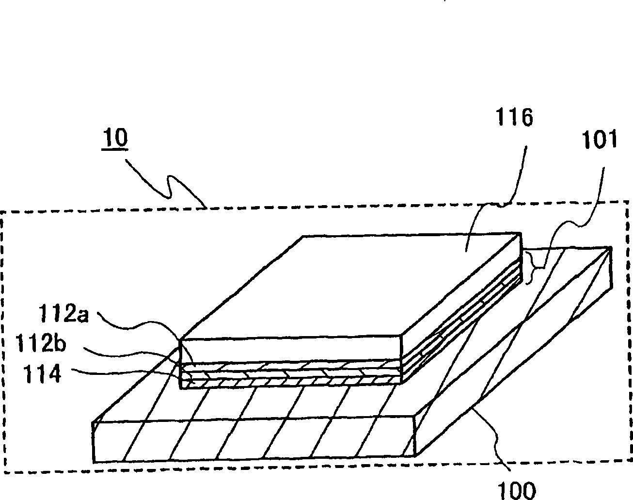
[0079] figure 1 is a perspective view showing a structural example of a semiconductor substrate. In the semiconductor substrate 10 , a single crystal semiconductor layer 116 is attached to the support substrate 100 . The single crystal semiconductor layer 116 is provided on the supporting substrate 100 via the buffer layer 101, and the semiconductor substrate 10 is a substrate having a so-called SOI structure in which a single crystal semiconductor layer is formed on an insulating layer.

[0080] The buffer layer 101 may have a single crystal structure or a multilayer structure in which two or more films are laminated. In this embodiment, the buffer layer 101 has a three-layer structure in which a bonding layer 114 , an insulating film 112 b , and an insulating film 112 a are laminated from the support substrate 100 side. The bonding layer 114 is formed of an insulating film. In addition, the insulating film 112a is an insulating film serving as a barrier layer. The barrie...

Embodiment approach 2

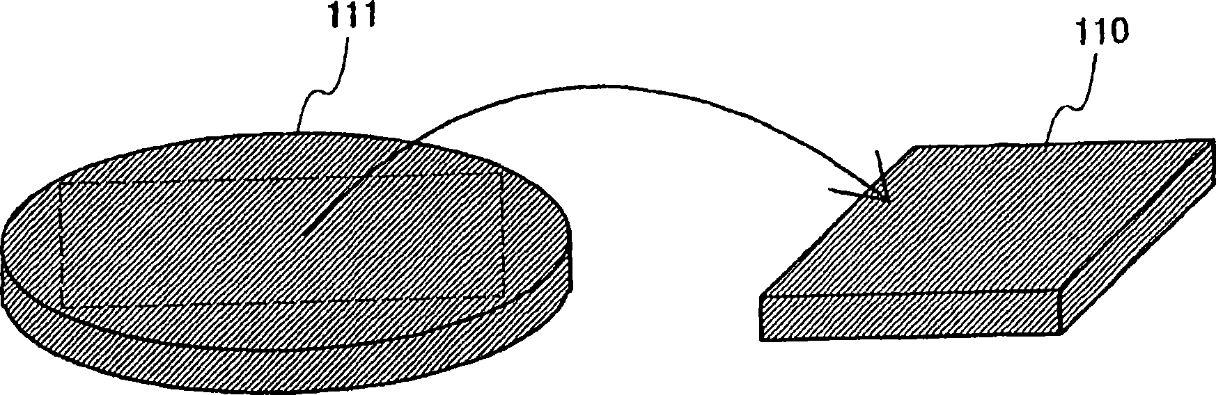
[0244] The single crystal semiconductor substrate 117 from which the single crystal semiconductor layer 115 has been separated can be regenerated and utilized as the single crystal semiconductor substrate 110 . In this embodiment, a regeneration treatment method will be described.

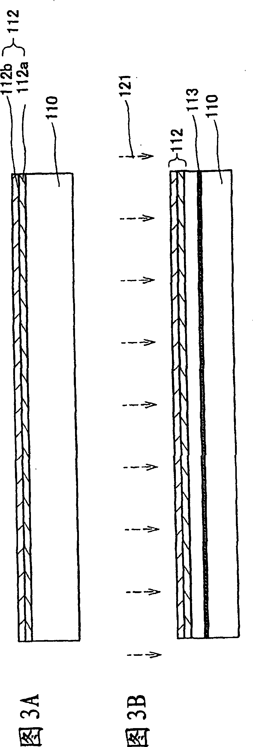
[0245] As shown in FIG. 4A , a portion not bonded to the supporting substrate 100 is left around the single crystal semiconductor substrate 117 . The insulating film 112b, the insulating film 112a, and the bonding layer 114 not attached to the support substrate 100 are left in this portion.

[0246] First, an etching process for removing the insulating film 112b, the insulating film 112a, and the bonding layer 114 is performed. For example, when these films are formed of silicon oxide, silicon oxynitride, or silicon oxynitride, the insulating film 112b, the insulating film 112a, and the bonding layer 114 can be removed by wet etching using a hydrofluoric acid aqueous solution.

[0247] Next, etch...

Embodiment approach 3

[0252] In this embodiment, refer to Figure 16A to Figure 18 , a method of manufacturing a transistor will be described as an example of a method of manufacturing a semiconductor device using the semiconductor substrate 10 . Various semiconductor devices are formed by combining a plurality of transistors. Below, refer to Figure 16A to Figure 18 A cross-sectional view illustrating how the transistor is fabricated. Note that, in this embodiment mode, a method of simultaneously manufacturing an n-channel type transistor and a p-channel type transistor will be described.

[0253] As shown in FIG. 16(A), the semiconductor film 603 and the semiconductor film 604 are formed by processing (patterning) the single crystal semiconductor layer on the supporting substrate 100 into a desired shape by etching. A p-type transistor is formed using the semiconductor film 603 , and an n-type transistor is formed using the semiconductor film 604 .

[0254] In order to control the threshold v...


PUM


Abstract

A semiconductor substrate including a single crystal semiconductor layer with a buffer layer interposed therebetween is manufactured. A semiconductor substrate is doped with hydrogen to form a damaged layer containing a large amount of hydrogen. After the single crystal semiconductor substrate and a supporting substrate are bonded, the semiconductor substrate is heated so that the single crystal semiconductor substrate is separated along a separation plane. The single crystal semiconductor layer is irradiated with a laser beam from the single crystal semiconductor layer side to melt a region in the depth direction from the surface of the laser-irradiated region of the single crystal semiconductor layer. Recrystallization progresses based on the plane orientation of the single crystal semiconductor layer which is solid without being melted; therefore, crystallinity of the single crystal semiconductor layer is recovered and the surface of the single crystal semiconductor layer is planarized.

Description

technical field [0001] The present invention relates to a method of manufacturing a semiconductor substrate on which a single crystal semiconductor layer is fixed via a buffer layer, a semiconductor device manufactured by the method, and electronic equipment including the semiconductor device. Background technique [0002] In recent years, research and development of integrated circuits using SOI (Silicon On Insulator, silicon on insulator) substrates instead of bulk silicon wafers has been carried out. By utilizing the characteristics of a thin single crystal silicon layer formed on an insulating layer, it is possible to form semiconductor layers of transistors in an integrated circuit completely separated from each other and make the transistors fully depleted. Therefore, a semiconductor integrated circuit with high added value such as high integration, high-speed drive, and low power consumption can be realized. [0003] As the SOI substrate, a SIMOX substrate and a bond...

Claims


Application Information

Patent Timeline
Patent Type & Authority Applications(China)
IPC IPC(8): H01L21/00H01L21/20H01L21/762H01L21/84H01L21/02H01L21/265H01L21/268H01L21/322H01L21/336H01L27/12H01L29/786
CPCH01L27/1214H01L27/1266H01L21/02532H01L21/76254H01L21/02686H01L29/66772H01L27/1218H01L27/1285H01L21/20
Inventor 下村明久井坂史人永野庸治桃纯平
Owner SEMICON ENERGY LAB CO LTD
Why Eureka
Try Eureka