Method for manufacturing semiconductor micro electromechanical structure

A technology of micro-electromechanical structure and manufacturing method, applied in micro-structure technology, micro-structure device, manufacturing micro-structure device and other directions, can solve the problems of pollution of micro-electro-mechanical structure, difficult to package, troublesome and complicated, and reduce the probability of damage, The effect of reducing the amount of etching and avoiding side etching

Inactive Publication Date: 2009-05-20
MEMSMART SEMICON
View PDF2 Cites 6 Cited by
  • Summary
  • Abstract
  • Description
  • Claims
  • Application Information

AI Technical Summary

Problems solved by technology

[0007] One is that it uses anisotropic dry chemical etching to remove the insulating layer material by means of chemical reaction. However, after passing through the side edges of the microelectromechanical structure, it is still necessary to perform isotropic chemical etching to remove the material. A large amount of silicon-based substrates are etched away, so this technology will cause serious undercuts;
[0008] The second is that in the process of this common technology, the MEMS structure is exposed to the process from the beginning. After a long period of multi-layer process processing, the MEMS structure is often polluted and damaged, resulting in a low yield;
[0009] The third is that after the etching operation is completed in this process technology, the MEMS structure can already operate in suspension, but the surface of the MEMS structure must be encapsulated with special mechanical tools to block the air, but since the MEMS structure must be guaranteed to be suspended In the past, a special mold cover was used to set the surface of the product, and then a packaging protective film that did not touch the suspended MEMS structure was precisely manufactured. However, this surface packaging technology is more complicated and costly, and it cannot be compared with the packaging of general integrated circuits. to integrate
[0010] The development of micro-electromechanical structure manufacturing technology is very rapid. In order to improve the above-mentioned problems, the US patent specification US6712983B2 (authorization date: March 30, 2004) proposed the use of ion etching (Reactive Ion Etching, hereinafter referred to as RIE) technology, which Although this technique can greatly reduce the undercut phenomenon (under cut), it is also etched layer by layer from top to bottom, and the last large amount of silicon substrate etching work must be achieved by lateral etching technology, so this The improved technology is too cumbersome and complicated, and there will still be under cut through a large amount of etching and lateral etching through the MEMS structure, and the above-mentioned problems that the MEMS structure is exposed and difficult to package have not yet been solved. improve

Method used


Image

  • Method for manufacturing semiconductor micro electromechanical structure
  • Method for manufacturing semiconductor micro electromechanical structure
  • Method for manufacturing semiconductor micro electromechanical structure

Examples


Embodiment Construction

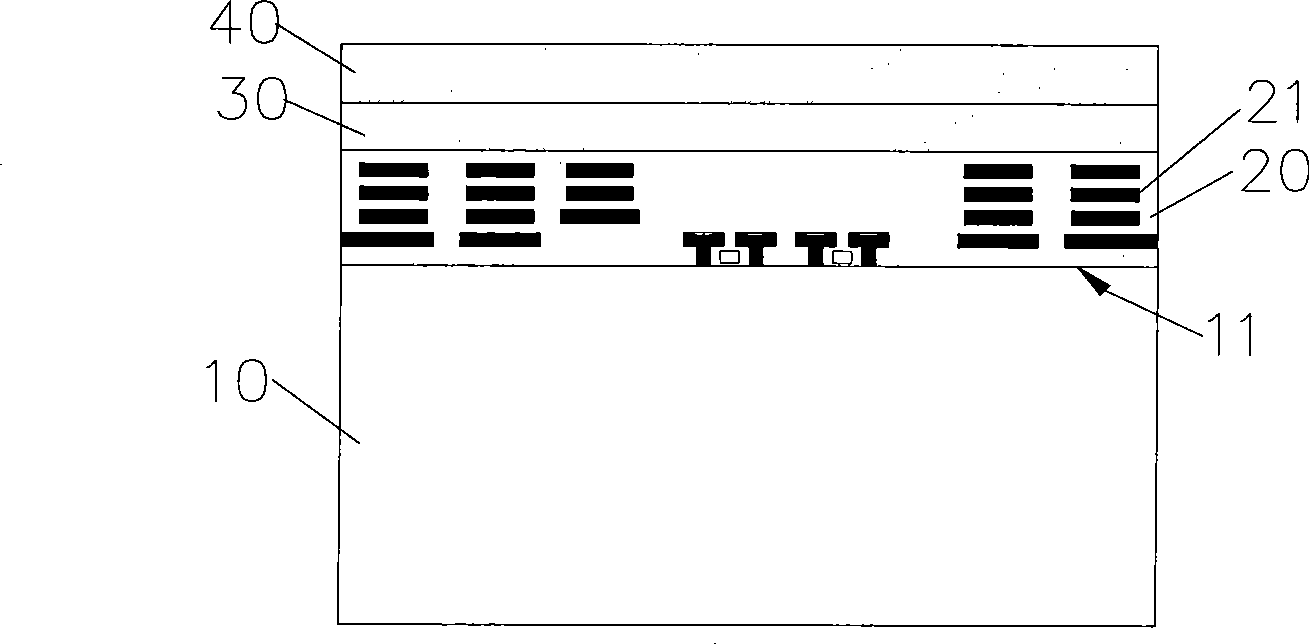
[0025] Figure 1 to Figure 5 The first embodiment of the manufacturing method of the semiconductor micro-electromechanical structure of the present invention is provided, and the specific steps are as follows:

[0026] (1) At first prepare at least one insulating circuit layer 20 with a micro-electromechanical structure 21 on the upper surface 11 of a silicon-based substrate 10, and make a sacrificial layer 30 and A barrier layer 40 (see figure 1 );

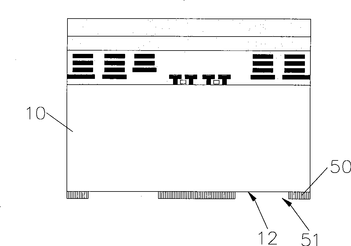
[0027] (2) Then make one layer of etch barrier layer 50 on the lower back surface 12 of the silicon base substrate 10, and etch the opening 51 of the barrier layer 50, the position of the opening 51 corresponding to the microelectromechanical structure 21 (see figure 2 );

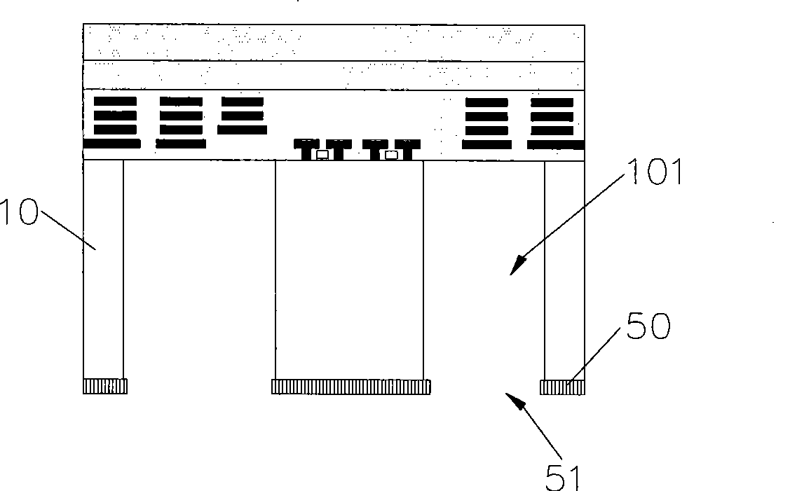
[0028] (3) Deep reactive ion etching (DRIE) or wet etching is carried out from the lower back surface 12 of the silicon-based substrate 10, and a space 101 corresponding to the micro-electromechanical structure 21 is oriented formed on the silicon-based su...


PUM


Abstract

The invention discloses a method for manufacturing a semiconductor micro electronmechanical structure, which comprises the steps: firstly, at least one insulation circuit layer internally provided with a micro electronmechanical structure is produced on the upper surface of a silicon substrate, and a sacrifice layer and a blocking layer are sequentially produced on the upper surface of the insulation circuit layer from interior to exterior; secondly, an etching blocking layer is made on the lower backface of the silicon substrate, and deep reactive ion etching or wet etching is carried out to the lower backface of the silicon substrate so as to form a space corresponding to the micro electronmechanical structure; and finally etching is carried out to the insulation circuit layer and the sacrifice layer in sequence to lead the micro electronmechanical structure to be suspended. Therefore, lateral erosion can be effectively avoided, the probability of exposure and damage of the micro electronmechanical structure is low, and the final encapsulation cost can be reduced by being integrated with common integrated circuit packaging technologies.

Description

technical field [0001] The invention relates to a method for manufacturing a semiconductor, in particular a method for manufacturing a semiconductor micro-electromechanical structure. Background technique [0002] Existing semiconductor microelectromechanical systems include various semiconductor microstructures, such as immovable probes, flow channels, and cavity structures, or some movable springs, connecting rods, and gears (rigid body motion or flexible deformation ) and other structures. [0003] Various semiconductor applications can be formed by integrating the above-mentioned different structures and related semiconductor circuits. Therefore, how to improve the various functions of the micro-mechanical structure through the manufacturing method is a key indicator of the future semiconductor MEMS, and it is also a severe challenge for further research on chips in the future. If the known technology can be developed and improved, the future development prospects cann...

Claims


Application Information

Patent Timeline
Patent Type & Authority Applications(China)
IPC IPC(8): B81C1/00
Inventor 陈晓翔刘政谚
Owner MEMSMART SEMICON
Why Eureka
Try Eureka