Optical approaching correction, photo mask production and graphic method

A technology of optical proximity correction and manufacturing method, which is applied in the field of optical proximity correction, can solve problems such as shrinkage and device short circuit, and achieve the effects of preventing bridging and solving short circuit phenomena

Active Publication Date: 2009-06-17
SEMICON MFG INT (SHANGHAI) CORP
View PDF1 Cites 14 Cited by
  • Summary
  • Abstract
  • Description
  • Claims
  • Application Information

AI Technical Summary

Problems solved by technology

[0007] Integrated circuits are generally divided into dense areas of semiconductor devices, sparse areas of semiconductor devices, and isolated areas of semiconductor devices. As the critical dimensions of semiconductor devices continue to decrease, the pitch between semiconductor devices is also shrinking. Therefore, contact holes in dense areas of semiconductor devices The distance between them is relatively short. After the optical proximity correction is performed on the layout contact hole pattern, the contact hole pattern transferred to the wafer on the photoresist may be bridged due to inappropriate correction amount, and then the subsequently formed Adjacent contact holes are connected to short circuit between devices

Method used


Image

  • Optical approaching correction, photo mask production and graphic method
  • Optical approaching correction, photo mask production and graphic method
  • Optical approaching correction, photo mask production and graphic method

Examples


Embodiment Construction

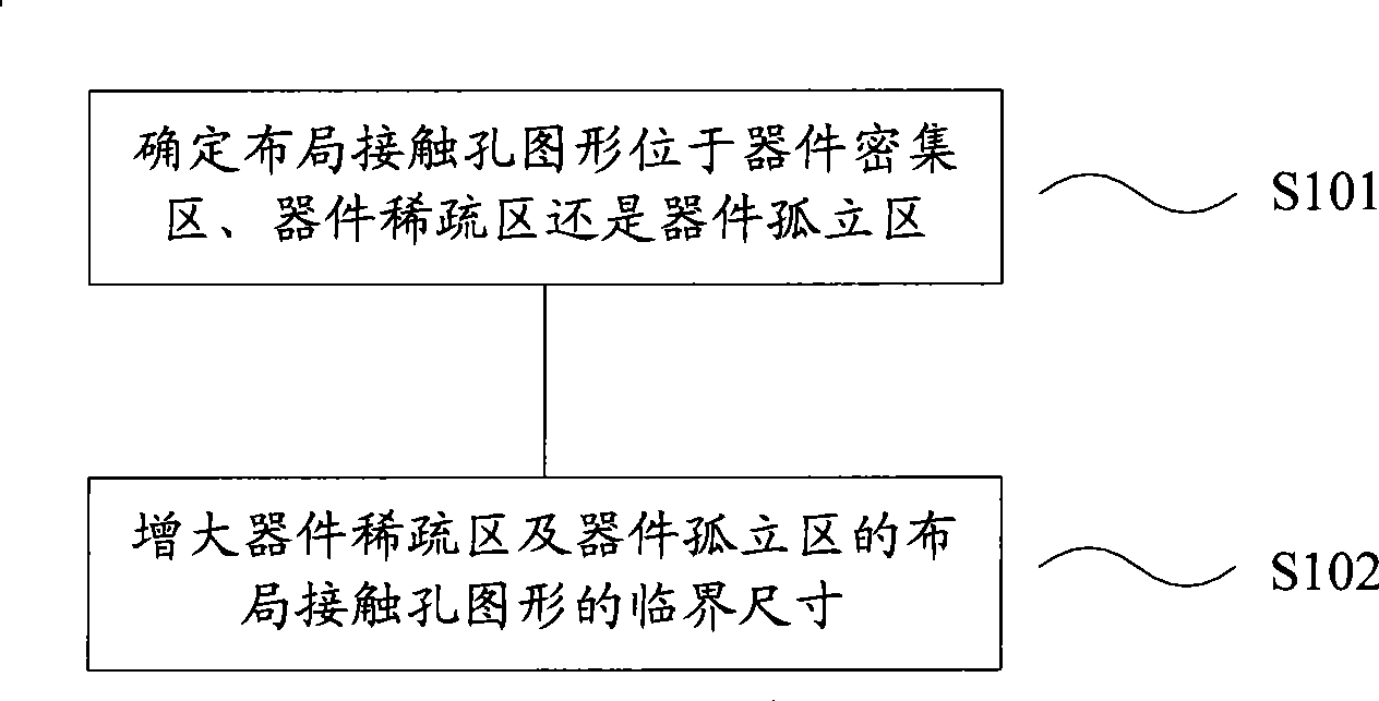
[0028] The present invention can selectively adjust the critical size of the layout contact holes in different regions by determining whether the layout contact hole pattern is located in the device dense area, the device sparse area or the device isolated area, and the layout contact hole pattern of the device sparse area and the device isolated area Increase the critical dimension of the wafer so that the subsequent contact holes formed on the wafer will not be lost because the critical dimension is too small. The increase of the contact hole causes the bridging between the contact holes, thereby effectively solving the short circuit phenomenon between the devices.

[0029] The specific embodiments of the present invention will be described in detail below in conjunction with the accompanying drawings.

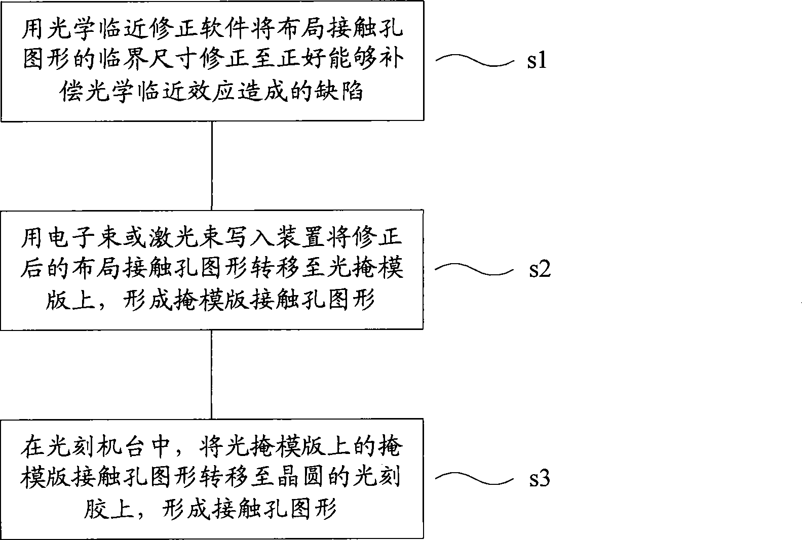
[0030] figure 2 It is a specific implementation flow chart of the optical proximity correction of the present invention. Such as figure 2 As shown, step S101 is execute...


PUM


Abstract

An optical approaching correction method comprises: determining that layout contact hole patterns are positioned in a device concentration area, a device sparse area and a device isolation area; and increasing critical dimensions of the layout contact hole patterns in the device sparse area and the device isolation area. The invention also provides a manufacturing method of a photomask plate and a graphical method thereof. The invention prevents bridge connection among the layout contact hole patterns caused by the concentration of devices and the increment of the critical dimensions, and further effectively solves short-circuit phenomenon among the devices.

Description

technical field [0001] The invention relates to the technical field of semiconductor manufacturing, in particular to an Optical Proximity Correction (OPC, Optical Proximity Correction) method, a photomask manufacturing method and a patterning method. Background technique [0002] With the rapid development of semiconductor manufacturing technology, in order to achieve faster computing speed, larger data storage capacity and more functions of semiconductor devices, semiconductor chips are developing towards higher integration. The higher the integration degree of the semiconductor chip, the smaller the critical dimension (CD, Critical Dimension) of the semiconductor device. [0003] However, due to the impact of the resolution limit of the optical exposure tool (optical exposure tool), the optical proximity effect (OPE) is likely to occur when performing an exposure process on these highly densely arranged photomask patterns for pattern transfer. , optical proximity effect),...

Claims


Application Information

Patent Timeline
Patent Type & Authority Applications(China)
IPC IPC(8): G03F1/14G03F1/00G03F1/36
Inventor 程仁强
Owner SEMICON MFG INT (SHANGHAI) CORP
Why Eureka
Try Eureka