

Method and device for wafer optimized scheduling
A technology that optimizes scheduling and wafers, and is used in control/regulation systems, program control, and overall factory control to achieve high benefits, reduce production costs, and reduce computing consumption.
- Summary
- Abstract
- Description
- Claims
- Application Information
AI Technical Summary
Problems solved by technology
Method used
Image

Examples
Embodiment Construction
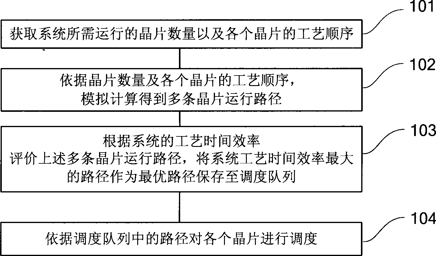
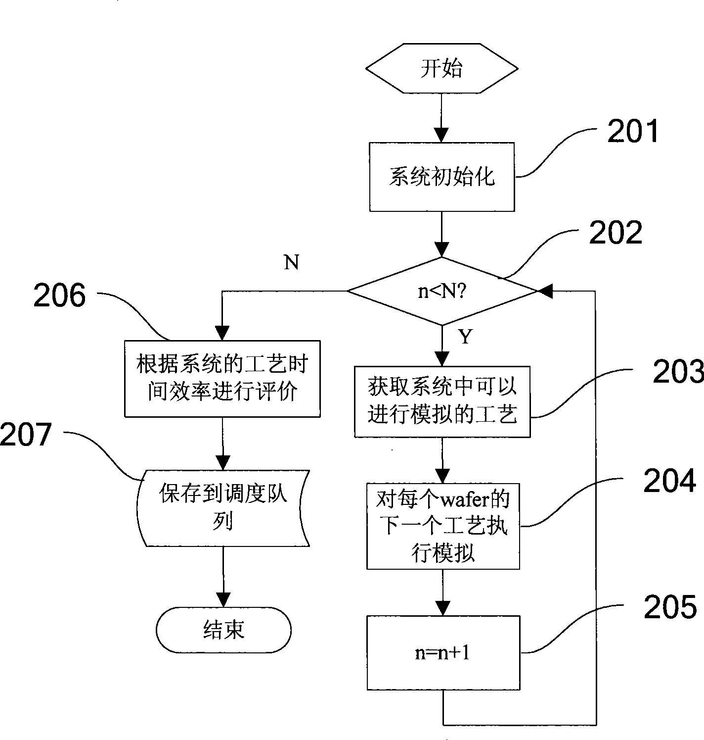
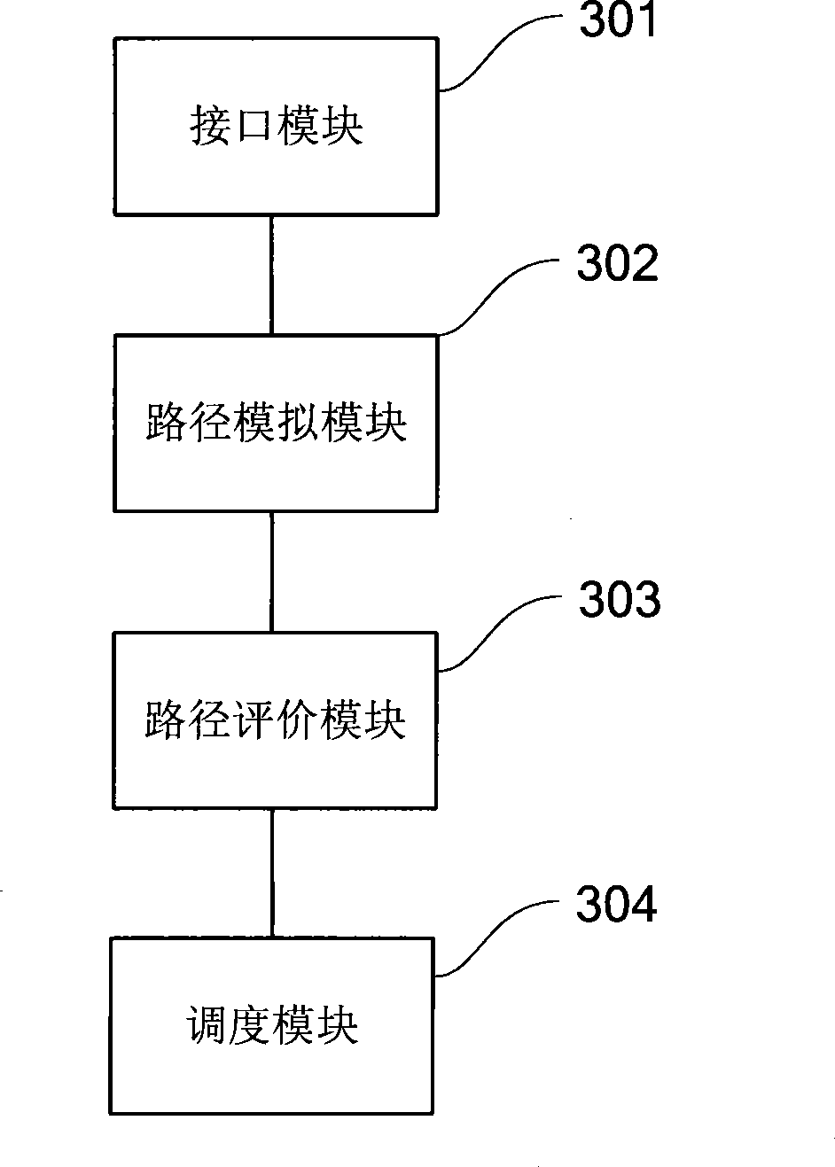
[0048] In order to make the above objects, features and advantages of the present invention more comprehensible, the present invention will be further described in detail below in conjunction with the accompanying drawings and specific embodiments.
[0049]The scheduling process flow of the present invention can run in many general-purpose or special-purpose computing system environments or configurations. For example: personal computers, server computers, handheld or portable devices, tablet-type devices, multiprocessor systems, microprocessor-based systems, network PCs, distributed computing environments including any of the above systems or devices, etc.
[0050] The invention may be described in the general context of computer-executable instructions, such as program modules, being executed by a computer. Generally, program modules include routines, programs, objects, components, data structures, etc. that perform particular tasks or implement particular abstract data type...
PUM
 Abstract
Description
Claims
Application Information