
Touch screen and display equipment

A technology for display devices and touch screens, which is applied in the fields of instruments, electrical digital data processing, nanostructure manufacturing, etc., can solve the problems of uneven resistance distribution, high ITO layer preparation cost, and decreased transparency, and achieve uniform resistance distribution and transparency. Optical properties, improved resolution and accuracy, good mechanical strength and toughness

Active Publication Date: 2009-06-24
TSINGHUA UNIV +1
View PDF0 Cites 7 Cited by
  • Summary
  • Abstract
  • Description
  • Claims
  • Application Information

AI Technical Summary

Problems solved by technology

[0005] However, as a transparent conductive layer, the ITO layer is usually prepared by ion beam sputtering or evaporation. During the preparation process, a high vacuum environment and heating to 200-300°C are required. Therefore, the preparation cost of the ITO layer is relatively high. high
In addition, as a transparent conductive layer, the ITO layer has disadvantages such as insufficient mechanical properties, difficulty in bending, and uneven resistance distribution.
In addition, the transparency of ITO will gradually decrease in humid air
As a result, existing resistive touch screens and display devices have shortcomings such as insufficient durability, low sensitivity, poor linearity and accuracy.

Method used


Image

  • Touch screen and display equipment
  • Touch screen and display equipment
  • Touch screen and display equipment

Examples


preparation example Construction

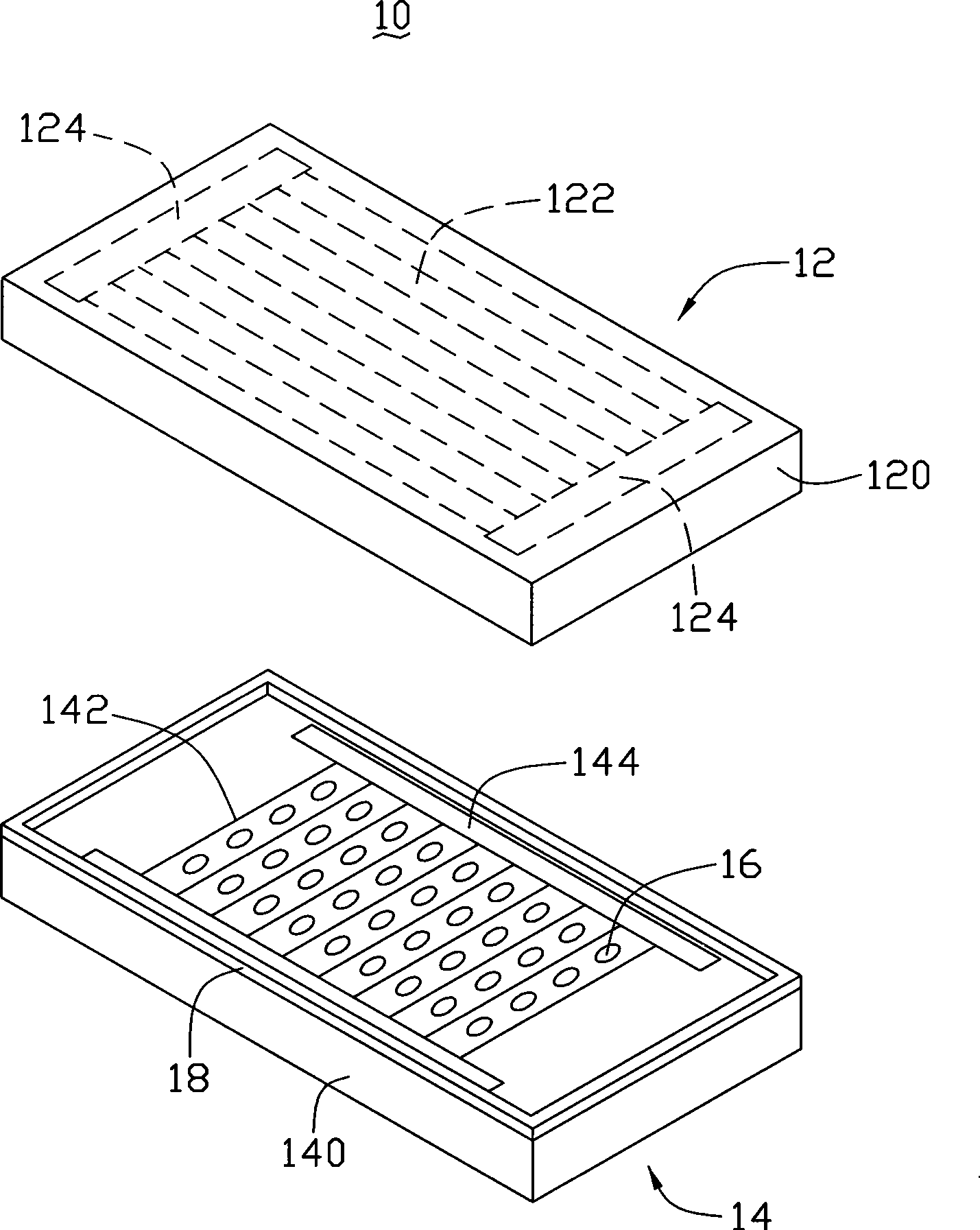
[0021] The preparation method of the first conductive layer 122 and the second conductive layer 142 described in the embodiment of the technical solution mainly includes the following steps:

[0022] Step 1: providing a carbon nanotube array formed on a substrate, preferably, the array is a superparallel carbon nanotube array.

[0023]The carbon nanotube array provided in the embodiment of the technical solution is one of a single-wall carbon nanotube array, a double-wall carbon nanotube array and a multi-wall carbon nanotube array. The preparation method of the carbon nanotube array adopts a chemical vapor deposition method, and its specific steps include: (a) providing a flat substrate, which can be a P-type or N-type silicon substrate, or a silicon substrate formed with an oxide layer. The embodiment preferably adopts a silicon substrate of 4 inches; (b) uniformly forms a catalyst layer on the surface of the substrate, and the catalyst layer material can be selected from ir...


PUM

PropertyMeasurementUnit
diameteraaaaaaaaaa
diameteraaaaaaaaaa
diameteraaaaaaaaaa

Abstract

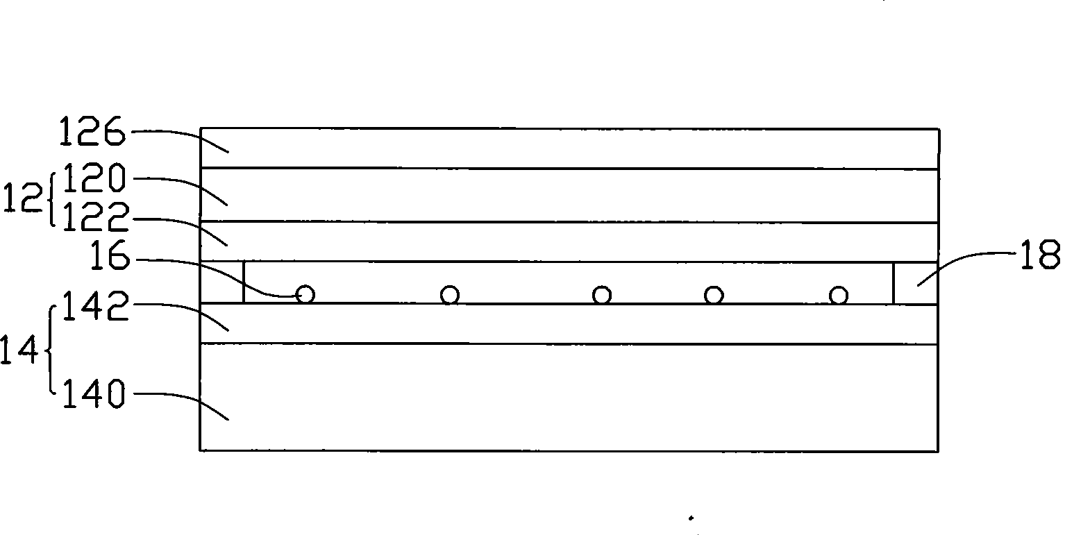
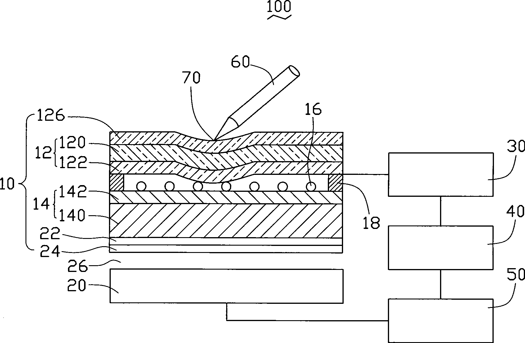
The invention relates to a touch screen, which includes a first electrode plate and a second electrode plate, wherein, the first electrode plate includes a first matrix and a first conducting layer arranged on the lower surface of the first matrix; the second electrode plate and the first electrode plate are arranged at internals; the second electrode plate includes a second matrix and a second conducting layer arranged on the upper surface of the second matrix; and at least one of the first conducting layer and the second conducting layer includes a plurality of parallel carbon nano tube long lines arranged at internals. The invention further relates to a display unit using the touch screen, which includes the touch screen and display equipment.

Description

technical field [0001] The invention relates to a touch screen and a display device using the touch screen, in particular to a carbon nanotube-based touch screen and a display device using the touch screen. Background technique [0002] In recent years, along with the high performance and diversification of various electronic devices such as mobile phones and touch navigation systems, there has been an increase in the number of electronic devices in which light-transmitting touch panels are mounted on the front of display elements such as liquid crystals. Users of such electronic devices operate by pressing the touch panel with fingers or a pen while visually confirming the display content of the display element located on the back of the touch panel through the touch panel. Thereby, various functions of the electronic device can be operated. [0003] According to different working principles and transmission media of touch screens, existing touch screens are usually divide...

Claims


Application Information

Patent Timeline
Patent Type & Authority Applications(China)
IPC IPC(8): G06F3/045H01H13/704B32B33/00B32B9/00B82B1/00
CPCG06F3/0412G06F3/045
Inventor 姜开利刘亮范守善
Owner TSINGHUA UNIV
Learn More