
Eureka
For R&D, Eureka makes reading and utilizing patents & technical documents easy.
Eureka AIR
Designed for self-driven R&D workflows. Generate viable solutions, solve complex R&D challenges, empower your innovation with AI.

Eureka Materials
Designed for material experts only. Revolutionize your material R&D, from search, analyze, to developing new materials.

TechResearch
Generate reliable direction feasibility study reports for your R&D in just a few steps.

TechSeek
Discover and master advanced knowledge NOW. Basics, ideas, possibilities, all at once.

TechMind
As an expert in R&D Theories, TechMind can generates customized viable solutions instantly.

TechRisk
Analyze your overall solution with one click, know your potential R&D risks in advance.

TechMonitor
Get weekly tech updates, stay abreast of the latest tech innovations and key insights.
Semiconductor light-emitting device
A light-emitting device and semiconductor technology, applied in the direction of semiconductor devices, electrical solid devices, electrical components, etc., can solve problems such as unexpectable welding strength, and achieve the effect of strong welding strength and low cost
- Summary
- Abstract
- Description
- Claims
- Application Information
AI Technical Summary
Problems solved by technology
Method used
Image

Examples
Embodiment 1
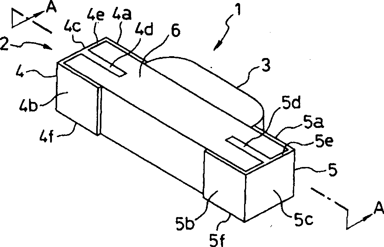
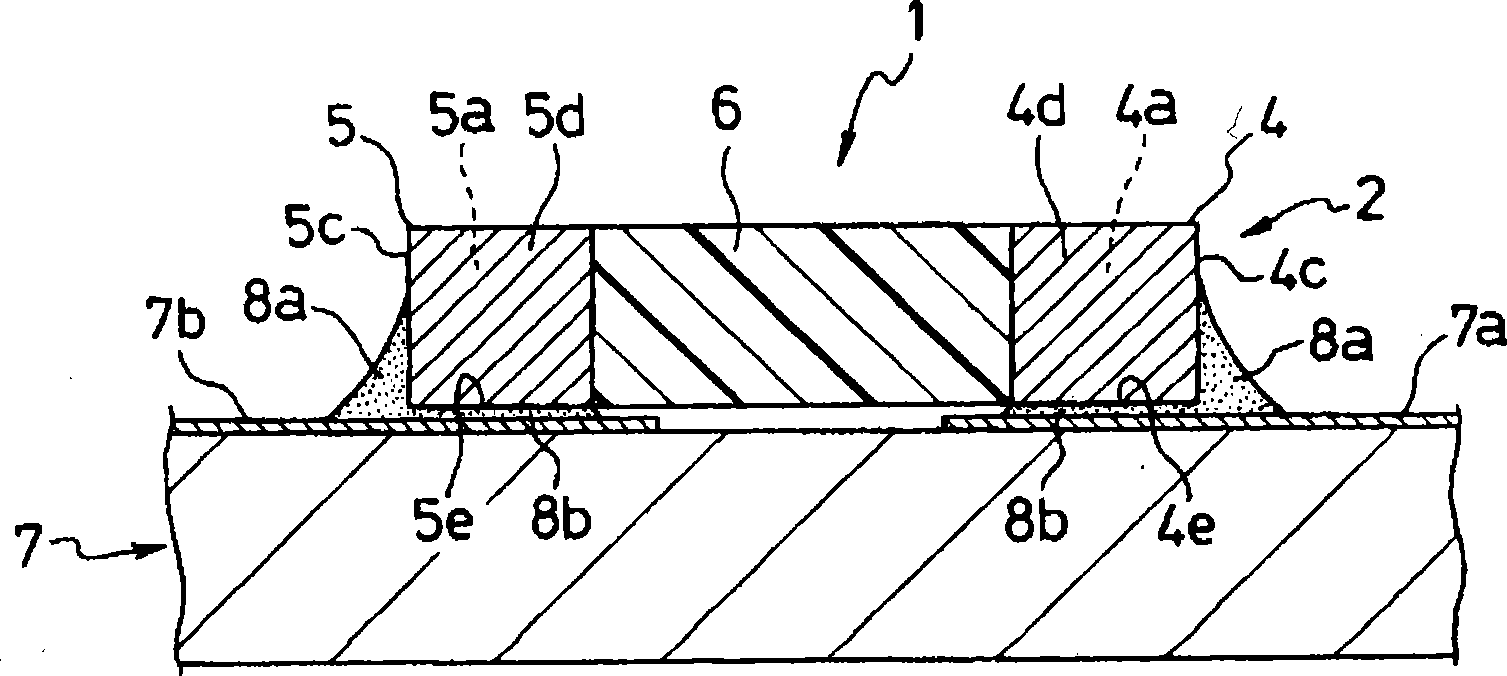
[0041] figure 1 It is a perspective view of Example 1 of the present invention, and is a view seen from the side opposite to the side on which the LED element is mounted and the side on which the circuit board is mounted. The side view type (side view type) LED lamp (hereinafter referred to as LED lamp) 1 of this embodiment is mainly composed of a substrate 2 for mounting LED elements, an LED element (not shown) and a sealing resin 3, and is made of a light-transmitting An LED lamp in which the LED element mounted on the LED element mounting substrate 2 is resin-sealed with a permanent sealing resin 3 . In addition, this Example is an Example in which one LED element was mounted.
[0042] Then, although not shown in the figure, an LED element is placed on one electrode 5 of a pair of electrodes 4, 5 on the LED element mounting substrate 2 via a conductive member to realize electrical conduction between the lower electrode of the LED element and the electrode 5. , and the up...
Embodiment 2
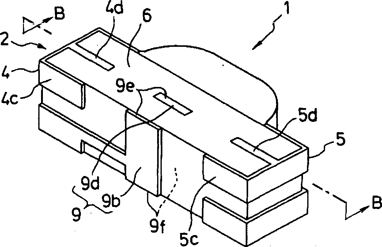
[0061] image 3 It is a perspective view of Example 2 of the present invention, and is a view seen from the side opposite to the side on which the LED element is mounted and the side on which the circuit board is mounted. This embodiment is an LED lamp equipped with 2 LED elements.
[0062] In this embodiment, compared with the above-mentioned embodiment 1, the electrode portion 9b and the electrode portion 9d are respectively located between the electrode portion 4c of the electrode 4 and the electrode portion 5c of the electrode 5 formed on the LED element mounting substrate 2 of the LED lamp 1, And between the electrode portion 4d of the electrode 4 and the electrode portion 5d of the electrode 5 . Moreover, the electrode part 9b and the electrode part 9d are connected in the insulating substrate 6, and the electrode 9 is comprised.
[0063] Generally, the electrode 9 is composed of a three-layer structure of copper foil layer / nickel plating layer / gold plating layer. lay...
Embodiment 3
[0068] Figure 5 It is a perspective view of Example 3 of the present invention, and is a view seen from the side opposite to the side on which the LED element is mounted and the side on which the circuit board is mounted.
[0069] In this embodiment, compared with the above-mentioned embodiment 1, on the end face 4e side near the electrode portion 4c of the electrode 4 formed on the LED element mounting substrate 2 of the LED lamp 1, a cross section penetrating through the electrode portion 4a and the electrode portion 4b is formed. Arc-shaped or elliptical groove portion 10 .
[0070] Similarly, on the side of the end surface 5e near the electrode portion 5c of the electrode 5 formed on the LED element mounting substrate 2 of the LED lamp 1, there is formed an arc-shaped or elliptical groove portion in cross section penetrating the electrode portion 5a and the electrode portion 5b. 11.
[0071] Both the groove part 10 and the groove part 11 are coated with a conductor on t...
PUM
 Abstract
Description
Claims
Application Information
 - R&D Engineer
- R&D Manager
- IP Professional
- Industry Leading Data Capabilities
- Powerful AI technology
- Patent DNA Extraction
Browse by: Latest US Patents, China's latest patents, Technical Efficacy Thesaurus, Application Domain, Technology Topic, Popular Technical Reports.
© 2024 PatSnap. All rights reserved.Legal|Privacy policy|Modern Slavery Act Transparency Statement|Sitemap|About US| Contact US: help@patsnap.com