

Thyristor controlled by accumulation layer
A technology of thyristor and accumulation layer, applied in the direction of thyristor, electrical components, circuits, etc., can solve the problems of current density limitation, reduction of forward voltage drop, increase of forward voltage drop, etc., to achieve low forward voltage drop, Large saturation current density, the effect of a wide range of applications
- Summary
- Abstract
- Description
- Claims
- Application Information
AI Technical Summary
Problems solved by technology
Method used
Image

Examples
Embodiment Construction
[0043] By adopting the accumulation layer control structure of the present invention, low conduction voltage drop, high current density, and large safe working area can be obtained, better current saturation characteristics and thyristor turn-off capability can be achieved, and it can be applied to epitaxial process and thin film process manufacturing technology . With the development of semiconductor technology, more power devices with low voltage drop, high current and high reliability can be produced by adopting the invention.
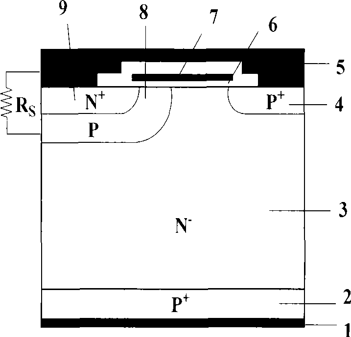
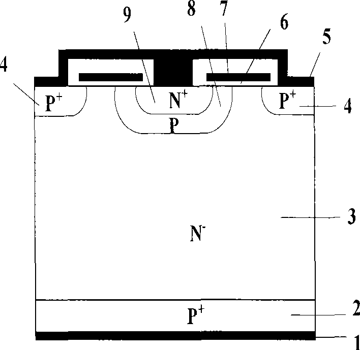
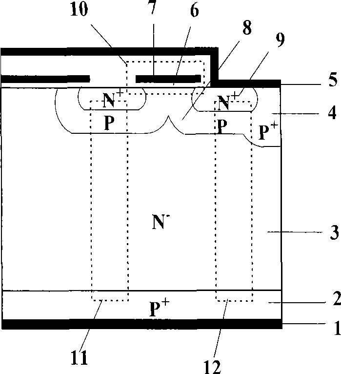
[0044] An accumulation layer controlled thyristor, such as Image 6 As shown, including metallized anode 1, anode P area 2, N - Base 3, P + Bypass region 4, metallized cathode 5, gate oxide layer 6, polysilicon gate 7, P-type base region 8, N + Source region 9, N - depletion region 33 and N + Layer 200; N - A trench insulating gate is sandwiched between the base region 3 and the metallized cathode 5, and the trench insulating gate is composed ...
PUM
 Abstract
Description
Claims
Application Information