
Thyristor controlled by accumulation layer

A thyristor, accumulation layer technology, applied in the direction of thyristor, electrical components, circuits, etc., can solve the problem of device turn-off capability and reliability limitations, gate-controlled thyristor has no large-scale application, device application scope limitations, etc., to achieve safe work. effect of increased area, improved turn-off capability, and low forward voltage drop

Inactive Publication Date: 2010-08-11
UNIV OF ELECTRONICS SCI & TECH OF CHINA
View PDF0 Cites 0 Cited by
  • Summary
  • Abstract
  • Description
  • Claims
  • Application Information

AI Technical Summary

Problems solved by technology

However, since the emitter turns off the thyristor, since the current flows through the MOS channel, the forward conduction voltage drop is larger than the forward conduction voltage drop of the above-mentioned MOS-controlled thyristor and the thyristor controlled by the base resistance, and once the thyristor works, the emission The positive safe operating area FBSOA (Forward Biased Safe Operating Area) of the pole-off thyristor is limited by the breakdown voltage of the surface MOSFET 10 (typically about 15 volts). In addition, the emitter-turn-off thyristor itself has a parasitic The thyristor, as shown in 12 in Figure 3, once the parasitic thyristor is turned on, the gate loses control, so its maximum controllable current density is limited, and the turn-off capability is greatly reduced
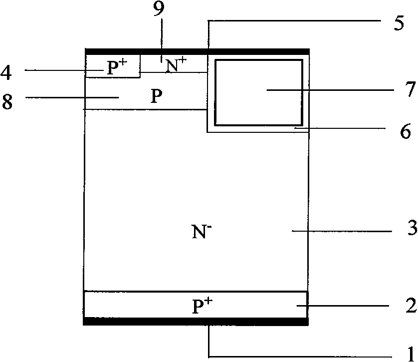
In order to improve the forward safe operating area of ​​the emitter turn-off thyristor structure, the literature M.S.Shekar, BJ.Baliga, M.Nandakumar, S.Tandon and AReisman, "High voltage current saturation in Emitter Switched Thyristors," IEEE Electron Device ktters, July 1991 , pp.387-389 proposed a dual-channel emitter-turn-off thyristor DC-EST (Dual Channel Emitter Switched Thyristor), as shown in Figure 4, this structure can obtain a better forward safe operating area, but At the same time, due to the introduction of the dual MOSFET structure 10, the forward conduction voltage drop of the device increases, and the parasitic thyristor 12 effect of the device itself has not been eliminated, so its maximum controllable current density is still limited, and the reliability needs to be further improved. improve
Subsequently, the document SRIDHA, S., BALIGA, B.J., "The dual gate emitter switched thyristor (DG-EST)".IEEE Electron Device Lett., 1996.17.(1).PP.25-27 proposed a dual gate emitter The DG-EST (Dual Gate Emitter Switched Thyristor) structure is shown in Figure 5. This structure is a composite structure of an emitter-off thyristor and a dual-channel emitter-off thyristor, combining two The advantages of the former make the device obtain a larger forward safe operating area while reducing the forward conduction voltage drop. However, the double gate control structure limits the application range of the device to a certain extent; on the other hand, as shown in Figure 5 The parasitic thyristor shown in 11 still exists, which limits the turn-off capability and reliability of the device
How to obtain the current saturation characteristics and effective and uniform turn-off capability of gate-controlled thyristors are two major problems that researchers have been exploring and trying to solve, and they are also important factors that have led to the large-scale application of gate-controlled thyristors.

Method used


Image

  • Thyristor controlled by accumulation layer
  • Thyristor controlled by accumulation layer
  • Thyristor controlled by accumulation layer

Examples


Embodiment Construction

[0043] By adopting the accumulation layer control structure of the present invention, low conduction voltage drop, high current density, and large safe working area can be obtained, better current saturation characteristics and thyristor turn-off capability can be achieved, and it can be applied to epitaxial process and thin film process manufacturing technology . With the development of semiconductor technology, more power devices with low voltage drop, high current and high reliability can be produced by adopting the invention.

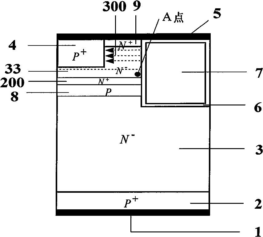
[0044] A thyristor controlled by an accumulation layer, as shown in Figure 6, includes a metallized anode 1, an anode P region 2, a N - Base 3, P + Bypass region 4, metallized cathode 5, gate oxide layer 6, polysilicon gate 7, P-type base region 8, N + Source region 9, N - depletion region 33 and N + Layer 200; N - A trench insulating gate is sandwiched between the base region 3 and the metallized cathode 5, and the trench insulating gate is co...


PUM


Abstract

An accumulation layer controlled thyristor, which belongs to the technical field of semiconductor power devices, is characterized in that the on / off of the thyristor can be controlled by stopping electron circulation through an electron barrier of an internal electric field formed in a P<+> bypass region and an N<-> depletion region. When a positive voltage is applied on a gate, an accumulation layer is formed at the interface between the N<-> depletion region (33) and a gate oxide layer (6); an electron inversion channel is formed in a P-type base region (8); and electrons pass through an N<+> active region (9), the accumulation layer, an N<+> layer (200), and the electron inversion channel to the an N<-> base region (3), thereby controlling the normal operation of the device. The accumulation layer controlled thyristor as the substitute of the conventional gate controlled thyristors, such as MOS controlled thyristors, has the advantages of lower conduction voltage drop, larger saturation current density, no parasitic effect, and greatly improved safety operation area, and can overcome the disadvantages of the conventional gate-controlled thyristors, such as the deficiency of current saturation characteristic and poor turn-off capability.

Description

technical field [0001] A thyristor controlled by an accumulation layer belongs to the technical field of semiconductor power devices. Background technique [0002] In recent years, the insulated gate bipolar transistor (Insulated Gate Bipolar Transistor, or IGBT) has been widely used due to the combination of simple driving circuit of MOSFET, high switching speed and high current density and low saturation voltage of bipolar power transistor. Wider and wider. However, the forward conduction voltage drop of the IGBT will become very large when the high voltage is applied, which is mainly due to the N - The base region is very thick, lightly doped N on the side close to the emitter - The base region cannot be effectively modulated in conductance. In the gate-controlled thyristor device, the anode has hole injection, and the cathode has electron injection, which can realize the N - The conductance modulation of the base area is sufficient, the forward voltage drop and on-st...

Claims


Application Information

Patent Timeline
Patent Type & Authority Patents(China)
IPC IPC(8): H01L29/74
CPCH01L29/7455
Inventor 李泽宏钱梦亮张波
Owner UNIV OF ELECTRONICS SCI & TECH OF CHINA
Learn More