High-speed test device

A testing device and high-speed technology, applied in the direction of measuring device, electronic circuit testing, measuring electricity, etc., can solve the problems of cost and man-hours, affecting the transmission characteristics of high-frequency signals, deformation of the probe card 12, etc., to reduce the production process, The effect of shortening the production period

Inactive Publication Date: 2009-07-22
MICROELECTRONICS TECH INC
View PDF1 Cites 12 Cited by
  • Summary
  • Abstract
  • Description
  • Claims
  • Application Information

AI Technical Summary

Problems solved by technology

[0003] by figure 1 Shown is the "semiconductor probe card for low current measurement" provided by US Patent No. 5808475. The structure of the probe card 1 is divided into an upper contact plate 10, a lower probe card 12, and several intervals in the middle material 14, wherein the contact circuit board 10 is provided with a test contact 11 with a coaxial transmission line structure, which can avoid the leakage current problem caused by the parasitic resistance generated by the medium environment of the contact circuit board 10 itself, but because the contact board 10 is directly for testing Touch the test head of the machine 1', and the probe board 12 is used to set the probes 13. If the contact board 10 or the probe board 12 itself does not have sufficient support strength and a certain rigid body thickness, when the test machine 1' is put down When pressing and applying stress to the entire structure of the probe card 1, the force-bearing plane of the contact plate 10 and the probe card 12 is likely to deform due to uneven local force. Moreover, when each probe 13 touches the chip plane, the front end of the individual probe card 12 needs to continuously bear the reaction force generated from the chip plane. Under such a long-term stress, the front end of the probe card 12 is used to set the probe 13 The planar structure is also prone to deformation
[0004] Even if figure 2 Shown is another commonly used probe card 2 structure, and its signal transmission process is through the circuit 21 laid on the multilayer printed circuit board 20 from outside to inside and from top to bottom extending through the laminated circuit board 20 , and then sent out by the probe 22, so the overall structural strength of the circuit board 20 and its single force-bearing plane can evenly disperse the force when it is under stress, without the problem of deformation caused by uneven local force; however, multi-layer printing The circuit board 20 is formed by laminating multiple layers of glass fiber material or ceramic material. Metal wires are arranged on each layer structure to form the structure of the wire 21. Therefore, not only considerable cost and man-hours are required to manufacture, but also the transmission line 21 When it is laid inside the circuit board, the material of the circuit board 20 between adjacent lines 21 is very likely to cause the main cause of leakage current, and the via hole line 210 pierced by each layer structure of the circuit board 10 is easy to cause the signal to be transmitted vertically The energy loss caused by interface reflection will seriously affect the transmission characteristics of high-frequency signals, and cannot meet the high-speed test requirements of electronic circuit components

Method used


Image

  • High-speed test device
  • High-speed test device
  • High-speed test device

Examples


Embodiment Construction

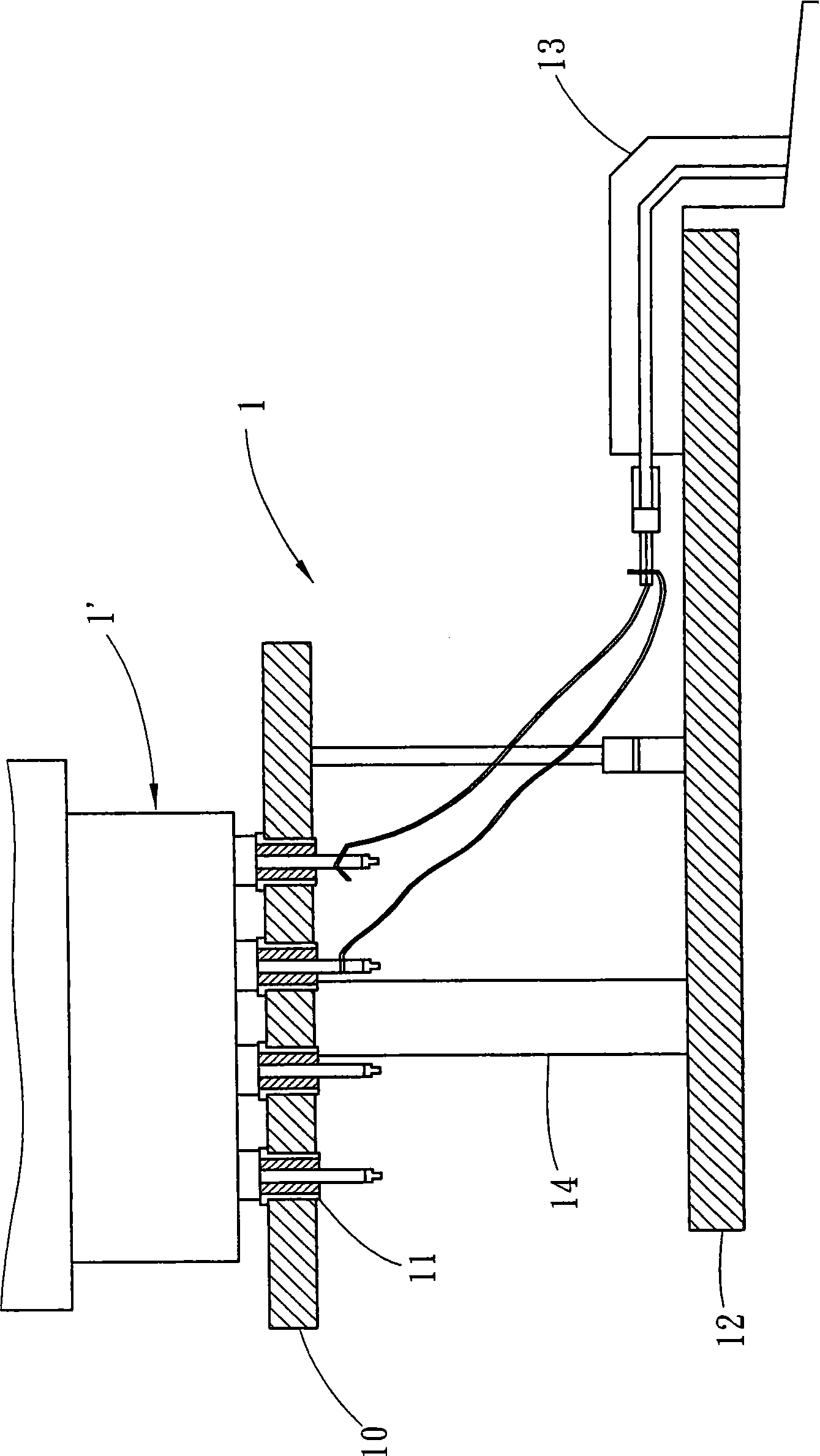
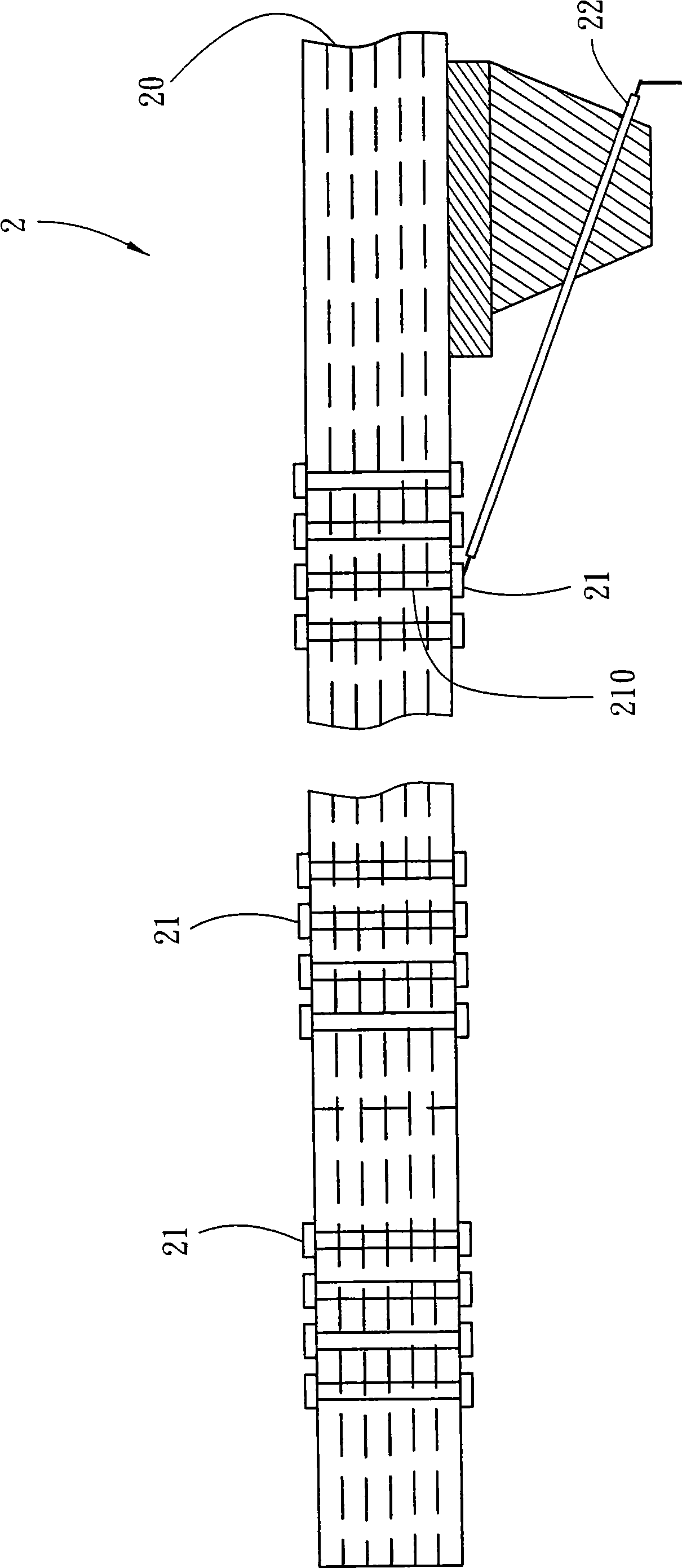
[0049] Hereinafter, some preferred embodiments are listed in conjunction with the diagrams, in order to describe the structure and effect of the present invention in detail, wherein the brief description of the diagrams used is as follows:

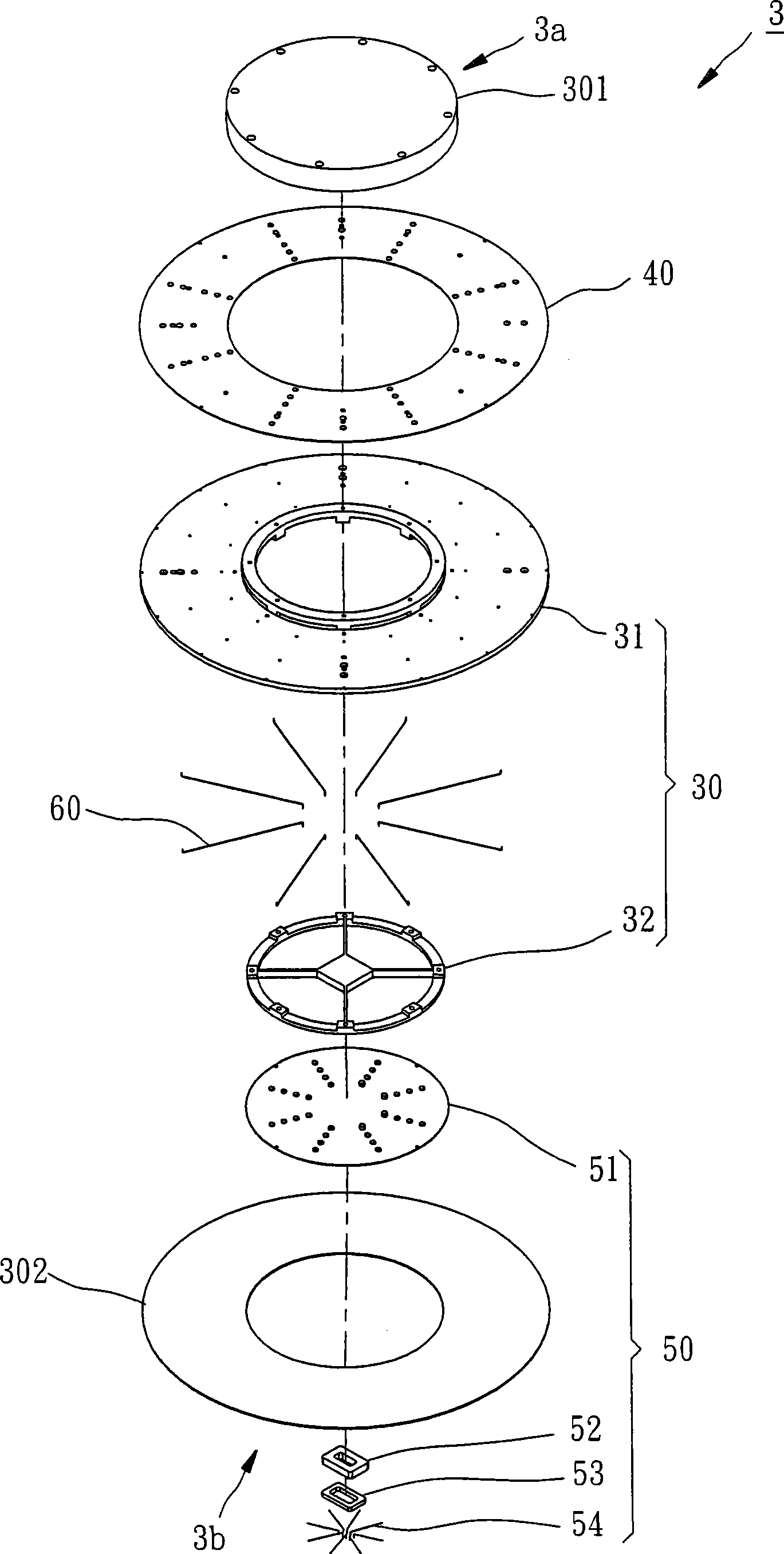
[0050] image 3 It is an exploded perspective view of the first preferred embodiment provided by the present invention;

[0051] Figure 4 It is a perspective view of the bottom of the first preferred embodiment above;

[0052] Figure 5 It is a structural schematic diagram of the above-mentioned first preferred embodiment;

[0053] Figure 6 It is a schematic bottom perspective view of the support frame provided by the first preferred embodiment above;

[0054] Figure 7 It is a combined top view of a part of the structure provided by the above-mentioned first preferred embodiment, and it is a schematic diagram of a combined structure with circuit layers, signal lines and probe sets arranged on the support frame;

[0055] Figure ...


PUM


Abstract

The invention discloses a high-speed test device, which is used for transmitting a test signal sent out by a test machine to electrically test an integrated circuit chip. A circuit layer and a probe set are arranged on and below a support frame respectively. When a lower pressure point of the test machine is contacted with the circuit layer and a corresponding point of the probe set is contacted with an electronic component on the chip, the support frame bears stress on upside and underside.

Description

technical field [0001] The invention relates to a testing device, in particular to a high-speed testing device for testing integrated circuit chips. Background technique [0002] In integrated circuit chip testing, the probe card circuit board used to transmit test signals is for the test head of the test machine to touch to receive the test signal of the test machine and transmit it to the densely arranged probes near the center of the circuit board. Above, when the chip electronic components touched by each probe receive the test signal, the corresponding electrical characteristics are sent back to the test machine through the probe card for analysis. In this way, during the entire chip-level test process, the probe card The circuit transmission design of the circuit board has a very important influence on the test results of the electronic components, especially as the electronic technology becomes more and more high-speed operation, the test process needs to operate unde...

Claims


Application Information

Patent Timeline
Patent Type & Authority Applications(China)
IPC IPC(8): G01R31/28G01R1/073
Inventor 顾伟正何志浩简志忠林合辉冯得诚赖俊良何家齐黄千惠张爱专
Owner MICROELECTRONICS TECH INC
Why Eureka
Try Eureka