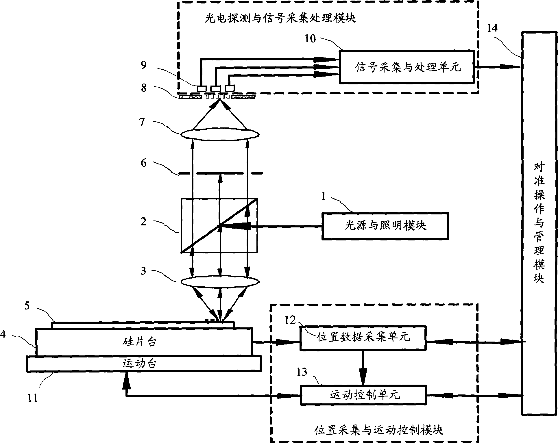
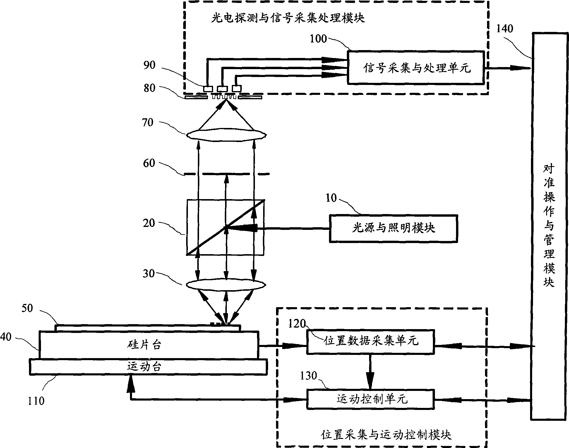
[0046] The system and method for capturing silicon wafer markers proposed by the present invention will be described in further detail below in conjunction with the accompanying drawings and specific embodiments.
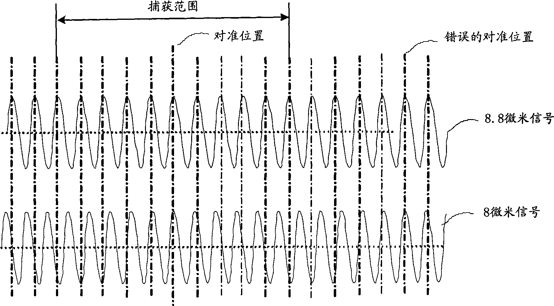
[0047] An embodiment of the present invention provides a silicon wafer mark capture system and method, which can ensure that the correct silicon wafer mark alignment position can be obtained even when the wafer on-chip repeat error exceeds the capture range of the silicon wafer alignment system , Thereby improving production efficiency.
[0048] In the process of engraving the silicon wafer, the lithography equipment first performs mechanical pre-alignment. If the on-chip repetition error of the silicon wafer exceeds the capture range of the silicon wafer alignment system of the lithography equipment, the mark pair cannot be accurately captured. Therefore, the silicon wafer mark capture system for lithography equipment is used to scan to obtain the position of the capture mark, and the position of the capture mark is used as a reference to indirectly realize the capture of the silicon wafer alignment mark. Ensure that the silicon wafer alignment system of the lithography equipment can perform the next fine alignment scan.
[0049] Please refer to image 3 , The silicon wafer mark capture system provided by an embodiment of the present invention includes: a light source and illumination module 10, an imaging module, a capture mark, a reference grating 80, a position acquisition and motion control module, a photoelectric detection and signal acquisition and processing module, and an alignment operation And management module 140; where the light source and illumination module 10, imaging module, reference grating 80, photodetection and signal acquisition and processing module, position acquisition and motion control module, alignment operation and management module 140 are shared with the silicon wafer alignment system , Thereby saving installation space and reducing production costs.
[0050] Wherein, the capture mark is arranged on the silicon wafer 5, the light source and the illumination module 10 provide an illumination beam to irradiate the capture mark to form diffracted light carrying the information of the capture mark, and the diffracted light is imaged by the imaging module The position acquisition and motion control module collects the position information of the motion platform 110 carrying the silicon chip 5, and provides the position information to the alignment operation and management module 140 to control the motion of the motion platform 110, the motion of the motion platform 110 Make the imaging of the capture mark scan the reference grating 80 and generate an optical signal; the photodetection and signal acquisition and processing module collects and processes the optical signal to generate a capture signal, and transmits the captured signal to the alignment operation and management module 140; The alignment operation and management module 140 determines the position of the capture mark according to the phase information and amplitude information of the capture signal.
[0051] Further, the light source and illumination module 10 provide at least one discrete wavelength of illumination light beams, for example, 633 nm and 532 nm. The illumination beam irradiates the capture mark of the silicon wafer 50 through the half mirror 20 and the front lens 30, and the corresponding order of diffracted light carrying the capture mark information is correlated and imaged on the reference grating 80 through the imaging module. The imaging module is a 4f imaging system, which includes a front lens group 30, a rear lens group 70, and a diaphragm 60 located between the front group lens 30 and the rear group lens 40. The diaphragm 60 is used to filter out unnecessary order. The diffracted light retains the diffracted light of the required order. The position acquisition and motion control module includes a position data acquisition unit 120 and a motion control unit 130. The position data acquisition unit 120 is used to collect position information of the sports station 110 and provide the position information to the alignment operation in real time. Together with the management module 140 and the motion control unit 130, the motion control unit 130 is used to control the motion table 110 to achieve linear reciprocating motion in the X or Y direction and high-precision positioning. Due to the uniform motion of the motion table 110, the imaging of the captured mark will scan through the reference grating 80, and the signal acquisition and processing will be performed by the photoelectric detection and signal acquisition and processing module. The photodetection and signal acquisition and processing module includes a photodetector 90 and a signal acquisition and processing unit 100. The photodetector 90 converts an optical signal into an electrical signal. The signal acquisition and processing unit 100 performs a fixed gain amplifying and amplifying the electrical signal. Discrete sampling processing, after processing into the captured signal, the captured signal is transmitted to the alignment operation and management module 140. The alignment operation and management module 140 determines the position of the capture mark according to the phase information and amplitude information of the captured signal, the phase information is the harmonic phase information of the captured signal, and the amplitude information is the Capture signal amplitude envelope information.
[0052] Please continue to refer Figure 4 , Among them, the shaded part is the wafer-on-chip repeat error range, and the size of the shaded area in the Y direction represents the silicon wafer's Y-chip repeat error range. The mark in the figure is a capture mark in the X direction, the capture mark includes a first grating branch P1 and a second grating branch P2, wherein the period of the first grating branch P1 is P10, and the period of the second grating branch P2 is P20 , There is a slight period difference between the first grating branch P1 and the second grating branch P2. In order to ensure that under the influence of the wafer loading repetition error, the capture mark can still be partially imaged on the reference grating, and the size of the grid bar of the capture mark in its extension direction is greater than or equal to the silicon wafer loading repetition error, that is, in the X direction The length of the capture mark in the extending direction of the grating strip is greater than or equal to the Y-direction silicon wafer loading repeat error. In addition, to ensure that the capture mark can be captured in one scan, the scan length should be greater than the wafer-on-chip repeat error. For example, the X-direction silicon wafer loading repeat error is about 300 microns, then the X-direction scan length can be set to 350 microns, so even if the X-up film error reaches the maximum value of about 300 microns, the X direction can still be captured by scanning. Capture mark.
[0053] Please continue to refer Figure 5 And combine Figure 3 to Figure 4The imaging of the capture mark is bright and dark stripes, and the reference grating 80 includes a first reference grating branch R1 and a second reference grating branch R2. During the scanning process, as the moving stage 110 moves at a constant speed, the capture mark is formed The light and dark stripes will scan through the first reference grating branch R1 and the second reference grating branch R2. The period of the first reference grating branch R1 is the same as the period of the light and dark fringe formed by P1, and the period of the second reference grating branch R2 is the same as the period of the light and dark fringe formed by P2. The fringe period is the same. The reference grating 80 includes light-transmissive and non-transmissive parts. A first photodetector is placed behind the first reference grating branch R1, and a second photodetector is placed behind the second reference grating branch R2. The optical signals of the reference grating branch R1 and the second reference grating branch R2.
[0054] The signal acquisition and processing unit 100 performs fixed gain amplification and discrete sampling processing on the optical signals obtained by the first photodetector and the second photodetector. Different scans can have different fixed gain values, but in each scan process, the signal gain value of each detector channel remains fixed from the beginning of the scan process to the end of the scan process to ensure that the gain is obtained during one scan. The alignment signal is amplified with the same gain.
[0055] Please continue to refer Figure 6 , Which is a schematic diagram of the signal when the number of reference gratings is not equal to the number of bright and dark fringes of the capture mark imaging. During the scanning process, the first photodetector obtains the capture signal S1, and the capture signal S1 has two obvious signal areas, namely the first capture The signal S1_1 and the third capture signal S1_2 respectively correspond to the signals when the imaging of the first grating branch P1 and the imaging of the second grating branch P2 of the capturing mark pass the first reference grating branch R1. The second photodetector obtains the capture signal S2. The capture signal S2 has two obvious signal areas, namely the fourth capture signal S2_1 and the second capture signal S2_2, which correspond to the imaging of the first grating branch P1 and the second grating branch of the capture mark, respectively. The image of P2 is the signal when the second reference grating branch R2 is scanned.
[0056] Since there is a slight difference between the period of the light and dark stripes of the second grating branch P2 and the period of the first reference grating branch R1, S2_1 is in the form of a sine-like signal instead of a standard sinusoidal signal. The period of the light and dark stripes of the first grating branch P1 is the same as that of the first reference grating branch R1. The period of the first reference grating branch R1 is the same, and S1_1 is a standard sinusoidal signal form. In the same way, the second photodetector after the second reference grating branch R2 obtains the signal S2. There are also two obvious signal areas S2_1 and S2_2 on the signal S2, which correspond to the imaging of the first grating branch P1 and the second grating that capture the mark. The imaging of branch P2 is the signal when the second reference grating branch R2 is scanned. Since the number of reference gratings is not equal to the number of bright and dark fringes of the captured mark imaging, the envelope of the signal area is trapezoidal. It should be noted that if the number of reference gratings is equal to the number of light and dark fringes of the captured mark imaging, the envelope of the signal area is a triangle. According to the start position of the scan and the scan length, in other embodiments of the present invention, The captured signal obtained can also be Figure 6 A segment of the signal shown in.
[0057] In the capture signal S1 and the capture signal S2, only the first capture signal S1_1 and the second capture signal S2_2 participate in the capture, that is, the imaging of the first grating branch P1 scans the signal obtained by scanning the first reference grating branch R1 at a constant speed, and the second grating The imaging of the branch P2 scans the signal obtained by scanning the second reference grating branch R2 at a constant speed to participate in the capture.
[0058] Please continue to refer Figure 7 And combine Figure 6 , The first capture signal S1_1 and the second capture signal S2_2 are two capture signals. By judging the threshold value, two signal areas in each signal can be obtained, and then according to the layout and scanning direction of the first reference raster branch R1 and the second reference raster branch R2, and the first raster branch P1 and the second raster branch that capture the mark The layout of branch P2 can easily extract S1_1 and S22 signal segments. The discrimination threshold can be set to half of the maximum value of the entire scanning signal, and signals larger than the threshold are obviously located in two areas, namely the signal area 1 greater than the threshold and the signal area 2 greater than the threshold. The layout of the reference raster is the first reference raster branch R1 and the second reference raster branch R2 from left to right, and the layout of the capture mark is the first raster branch P1 and the second raster branch P2 from left to right, and the scanning direction is from From left to right, then the obtained first capture signal S1_1 is in the latter signal area in the capture signal S1, and the second capture signal S2_2 is in the previous signal area in the capture signal S2.
[0059] In the silicon wafer mark capturing method provided by an embodiment of the present invention, an illumination beam is irradiated on the capturing mark; the imaging of the capturing mark scans a reference grating and generates an optical signal; and the optical signal is collected and processed to generate Capturing a signal; and determining the position of the capturing marker by the peak coincidence points included in the phase information of the capturing signal and the extreme points included in the amplitude information, wherein the phase information is the harmonic of the capturing signal Phase information, where the amplitude information is the amplitude envelope information of the captured signal. The silicon wafer mark capturing method provided by an embodiment of the present invention specifically includes the following steps:
[0060] Step 1. Set the start position and end position of the scan;
[0061] Step 2: Obtain the light intensity discrete signal after scanning, and extract the first capture signal S1_1 and the second capture signal S2_2;
[0062] Step 3: Perform phase fitting on the first captured signal S1_1 and the second captured signal S2_2 respectively to obtain the harmonic phase information of the first captured signal S1_1 and the second captured signal S2_2, and further obtain the peak value of the first captured signal S1_1 Point and the peak point of the second capture signal S2_2;
[0063] Step 4: Determine the peak coincidence point of the first capture signal S1_1 and the second capture signal S2_2 according to the peak point of the first capture signal S1_1 and the peak point of the second capture signal S2_2;
[0064] Step 5. Extract the envelope of the first capture signal S1_1 and the envelope of the second capture signal S2_2 according to the peak point of the first capture signal S1_1 and the peak point of the second capture signal S2_2;
[0065] Step 6. Obtain the moving average signal of the first captured signal S1_1 and the moving average signal of the second captured signal S2_2, and respectively fit the moving average signals to obtain the extreme points of the first captured signal S1_1 and the second Capture the extreme point of signal S2_2;
[0066] Step 7. Combining the extreme points of the capture signal and the peak coincidence point, determine the location of the capture mark, and use the location of the capture mark as a reference to realize the capture of the silicon wafer alignment mark.
[0067] In detail, the silicon wafer mark capturing method provided by an embodiment of the present invention includes the following processes:
[0068] First of all, the start position and end position of the scan are set to ensure that the actual position of the capture mark is covered, and the scan length is greater than the repetition error on the wafer. Wherein, the repetition error of the silicon wafer loading means that after the silicon wafer pre-alignment, the silicon wafer will be placed on the silicon wafer stage for the next step of processing, that is, the silicon wafer fine alignment will be performed, and the silicon wafer pre-aligned There is an alignment error, that is, there is an error between the actual position of the silicon wafer and the measured position obtained through pre-alignment. This error is the silicon wafer loading repeat error, that is, the multiple loading pre-alignment in the statistical sense. Quasi-error.
[0069] Then, perform phase fitting on the first captured signal S1_1 and the second captured signal S2_2 to obtain the harmonic phase information of the first captured signal S1_1 and the second captured signal S2_2, and further obtain the peak point of the first captured signal S1_1 and The peak point of the second capture signal S2_2. The fitted model can adopt any of the following cosine models:
[0070] (Formula 1)
[0071] (Equation 2)
[0072] (Equation 3)
[0073] Among them, I(x) represents the signal strength at position x, and p i Is the period of the signal. For the first capture signal S1_1, the period of the signal is the period of imaging of the first grating branch P1, and for the second capture signal S2_2, the period of the signal is the period of imaging of the second grating branch P2. a 1 , A 2 , A 3 , A 4 , A 5 , A 6 Is the polynomial parameter to be fitted, Is the phase parameter to be fitted. Use least squares or Newton iteration method to easily solve a i with value. In order to ensure the accuracy of the fitting, the signal segments participating in the fitting in the first capture signal S1_1 and the second capture signal S2_2 may be the middle part, or the signal segment with the amplitude greater than the discrimination threshold.
[0074] According to the fitting a i with Value, which can determine the peak point of the signal, that is When, the corresponding signal sampling point near the x coordinate. From the parameters obtained by fitting the two captured signals, it is possible to calculate the point where the peak positions of the first captured signal S1_1 and the second captured signal S2_2 completely coincide, or the point where the peak positions are closest.
[0075] Secondly, the amplitude fitting is performed on the first capture signal S1_1 and the second capture signal S2_2 to obtain the amplitude information of the first capture signal S1_1 and the second capture signal S2_2. On the first captured signal S1_1 and the second captured signal S2_2, the peak points of the signal constitute the envelope of the captured signal. The moving average signals of the envelopes of the first capture signal S1_1 and the second capture signal S2_2 are obtained respectively, and a signal in the form of a parabola is obtained. Such as Figure 8 As shown, the solid points are the peak points of the original signal, and the hollow points are the signals after moving average. The moving average signal is obtained using the following moving average method:
[0076] L ( x ) = Σ i = 0 k - 1 I ( x - kΔt ) k (Equation 4)
[0077] Among them, I(x) represents the signal strength at position x, k is the number of points involved, Δt is the interval between two sampling points, kΔt is the moving average window length, and L(x) is the x position after moving average The signal strength.
[0078] The signal after the moving average is fitted, and the fitting model adopts a parabolic model, namely:
[0079] L(x)=b 0 +b 1x +b 2 x 2 (Equation 5)
[0080] Among them, L(x) is the moving average signal strength at position x, b 0 , B 1 , B 2 , Is the parabola parameter to be fitted. By the least square method, b can be easily obtained 0 , B 1 , B 2 ,value. Then, the extreme point of the parabola is x = - b 1 2 b 2 Place.
[0081] Please continue to refer Picture 9 , The first capture signal S1_1 and the second capture signal S2_2 can respectively obtain a parabolic extreme point. The first capture signal S1_1 and the second capture signal S2_2 that are closest to the two extreme points are the coincidence points of the phase signals The location of the mark.
[0082] Please continue to refer Picture 10 , The phase fitting signals of the first capture signal S1_1 and the second capture signal S2_2 have multiple peak coincidence points, including the first peak coincidence point A, the second peak coincidence point B, and the third peak coincidence point C. The first capture The amplitude fitting signals of the signal S1_1 and the second capture signal S2_2 each have an extreme point, that is, the extreme point a of the first capture signal S1_1 and the extreme point b of the second capture signal S2_2. Obviously, the distance from the first capture signal The position of the second peak coincidence point B at the closest position of the extreme value point a of S1_1 and the extreme value point b of S2_2 is the position where the mark is captured, that is, the position where the mark can be captured.
[0083] In an embodiment of the present invention, the capture mark and the silicon wafer alignment mark are exposed on the silicon wafer through a mask, and the positional relationship between the capture mark and the silicon wafer alignment mark is fixed and known, and the position of the capture mark is obtained. Then, the position of the capture mark is used as a reference, so that the silicon wafer alignment mark can be captured indirectly, which can ensure that the mark alignment position is captured accurately and quickly.
[0084] In addition, due to errors such as manufacturing and assembly in practice, the peak points of the two captured signals may not completely coincide, and a series of peak points among them can be found. According to actual conditions, the extreme point may be the extreme point of the first captured signal, the extreme point or the extreme point of the second captured signal, and the extreme point may also be the The average value of the extreme point of the first captured signal and the extreme point of the second captured signal.
[0085] In summary, in the silicon wafer mark capture system and method provided by the present invention, the capture signal is obtained by scanning the reference grating through the imaging of the capture mark, and the capture signal is determined by the phase information and amplitude information of the capture signal. The position of the mark to achieve a wide range of capture of the mark alignment position after loading, which can ensure that the mark alignment position can be accurately and quickly achieved when the pre-alignment error of the loading exceeds the capture range of the silicon alignment system Therefore, the production efficiency is improved, and each module of the silicon wafer mark capturing system is shared with the silicon wafer alignment system, which saves installation space and reduces production costs.
[0086] Obviously, those skilled in the art can make various changes and modifications to the present invention without departing from the spirit and scope of the present invention. In this way, if these modifications and variations of the present invention fall within the scope of the claims of the present invention and their equivalent technologies, the present invention is also intended to include these modifications and variations.