Supercharge Your Innovation With Domain-Expert AI Agents!

Wafer bearing device

A carrier device and wafer technology, applied in the manufacture of electrical components, circuits, semiconductors/solid-state devices, etc., can solve problems such as disconnection, out-of-focus, poor graphics, etc., to improve the manufacturing pass rate, reduce contact stress, and avoid breakage line effect

Inactive Publication Date: 2009-07-29
VISERA TECH CO LTD
View PDF0 Cites 4 Cited by
  • Summary
  • Abstract
  • Description
  • Claims
  • Application Information

AI Technical Summary

Problems solved by technology

Then, when the wafer carrier 1 is transported together with multiple wafers, debris from the wafer carrier 1 from the support rods 11 tends to fall onto the surface of the wafer or onto the manufacturing equipment, thus causing the wafers to be lost during subsequent processing. bad phenomenon of damage
For example, as far as the debris from the wafer carrier falls onto the upper surface of the wafer, after the die on the wafer is exposed, some wiring on the surface will be damaged by the debris from the wafer carrier. There is a phenomenon of blocking light exposure, which will cause poor exposure of the pattern of the grain
On the other hand, in terms of the debris of the wafer carrier falling onto the lower surface of the wafer, when the lower surface of the wafer is adsorbed on a flat wafer chuck (wafer chuck) for exposure processing, the chip carrier is broken. The presence of debris will cause the exposed area on the wafer to protrude, which will cause local defocus in the exposed area, and in turn will cause some graphics on the surface of the grain to fail due to defocus
[0005] In addition, the large contact stress generated between the wafer W and the two support rods 11 of the strip structure will be further transmitted to the center and other parts of the wafer W, so the wiring on the crystal grains will also be affected by the stress. Existence and disconnection, which will also cause bad grain failure

Method used


Image

  • Wafer bearing device
  • Wafer bearing device
  • Wafer bearing device

Examples


Embodiment Construction

[0026] Preferred embodiments of the present invention are described below with reference to the accompanying drawings.

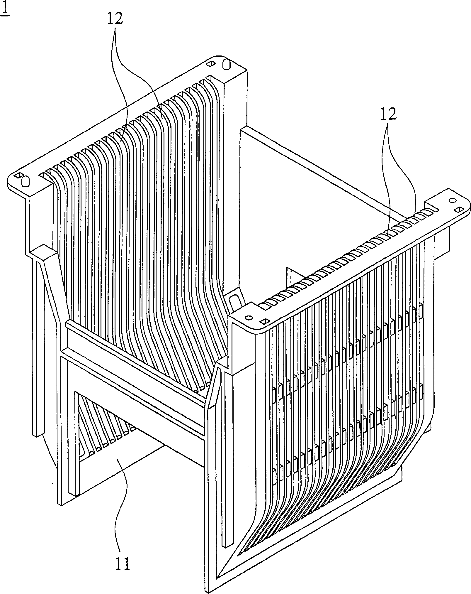
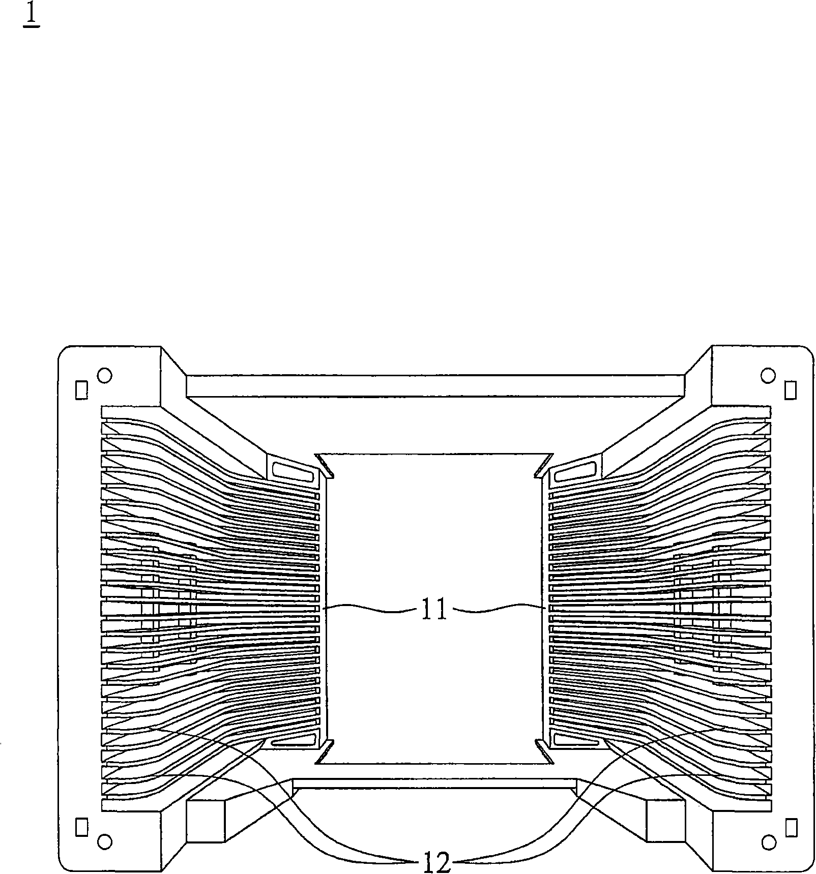
[0027] see Figure 3A and Figure 3B The wafer carrying device 100 of this embodiment may be made of PP or PEEK, etc., and mainly includes two opposite support rods 110 and a plurality of partition plates 120 .

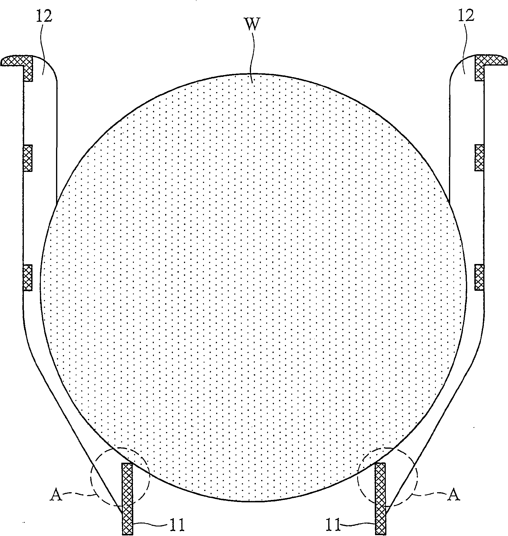
[0028] Such as Figure 3B As shown, each support rod 110 has a multiple arc-shaped resisting portion 111 . In more detail, as Figure 4 As shown, each multi-arc abutting portion 111 has a first arc surface 111a, a second arc surface 111b and a third arc surface 111c, and the second arc surface 111b is connected to the first arc surface 111a and the third arc surface between faces 111c. In particular, the curvature direction of the second arc surface 111b is opposite to that of the first arc surface 111a, and the curvature direction of the third arc surface 111c is the same as that of the first arc surface 111a. In this embodiment, the shapes o...


PUM


Abstract

The invention provides a wafer bearing device comprising at least one supporting bar and a plurality of separating panels. The supporting bar is provided with a multi-arc supporting part; the separating panels are connected to the multi-arc supporting part and arranged parallel and alternatively. The wafer bearing device maintains a fixed contact area between the multi-arc supporting part and the wafer, which can effectively reduce the contact stress between the multi-arc supporting part (or a supporting bar) and the wafer, thus significantly reducing chippings produced by the wafer bearing device, preventing the wires on the crystalline grain from breaking due to the existence of the stress, and then increasing the overall qualification rate of the wafer.

Description

technical field [0001] The invention relates to a wafer carrying (crystal boat) device, in particular to a wafer carrying device for carrying and transporting wafers. Background technique [0002] Generally speaking, in the semiconductor manufacturing process, the transportation of wafers is usually accomplished by a wafer carrier device (cassette). That is to say, a plurality of wafers can be carried by a wafer carrier, and transported by the wafer carrier to predetermined manufacturing equipment or destinations for subsequent manufacturing processes. [0003] see Figure 1A and Figure 1B , a conventional wafer carrier device 1 is usually made of PP or PEEK or other materials, and it mainly includes two opposite support rods 11 and a plurality of partition plates 12 . The plurality of partition plates 12 are respectively connected to the two support rods 11 , and the plurality of partition plates 12 are arranged parallel to and spaced apart from each other. When the waf...

Claims


Application Information

Patent Timeline
IPC IPC(8): H01L21/673
Inventor 郭养国邓国星李晨钟
Owner VISERA TECH CO LTD
Features
  • R&D
  • Intellectual Property
  • Life Sciences
  • Materials
  • Tech Scout
  • Unparalleled Data Quality
  • Higher Quality Content
  • 60% Fewer Hallucinations
Learn More