
Method for removing fluorine residue in manufacture process of semi-conductor

A semiconductor and process technology, applied in the field of removing fluorine residues in semiconductor manufacturing processes, can solve the problems of wafer crystal defects and fluorine residues have no special effect, and achieve the effect of avoiding crystal defects

Inactive Publication Date: 2009-08-05
SEMICON MFG INT (SHANGHAI) CORP +1
View PDF0 Cites 0 Cited by
  • Summary
  • Abstract
  • Description
  • Claims
  • Application Information

AI Technical Summary

Problems solved by technology

But when AL(OH) 3 By F - Continuous consumption, AL will continue to decompose, so the wafer will cause crystal defects (pad crystaldefect)
[0007] In the semiconductor manufacturing process, the existing cleaning method is mainly to remove particles, but has no special effect on the fluorine residue of related components

Method used


Image

  • Method for removing fluorine residue in manufacture process of semi-conductor
  • Method for removing fluorine residue in manufacture process of semi-conductor
  • Method for removing fluorine residue in manufacture process of semi-conductor

Examples


Embodiment 1

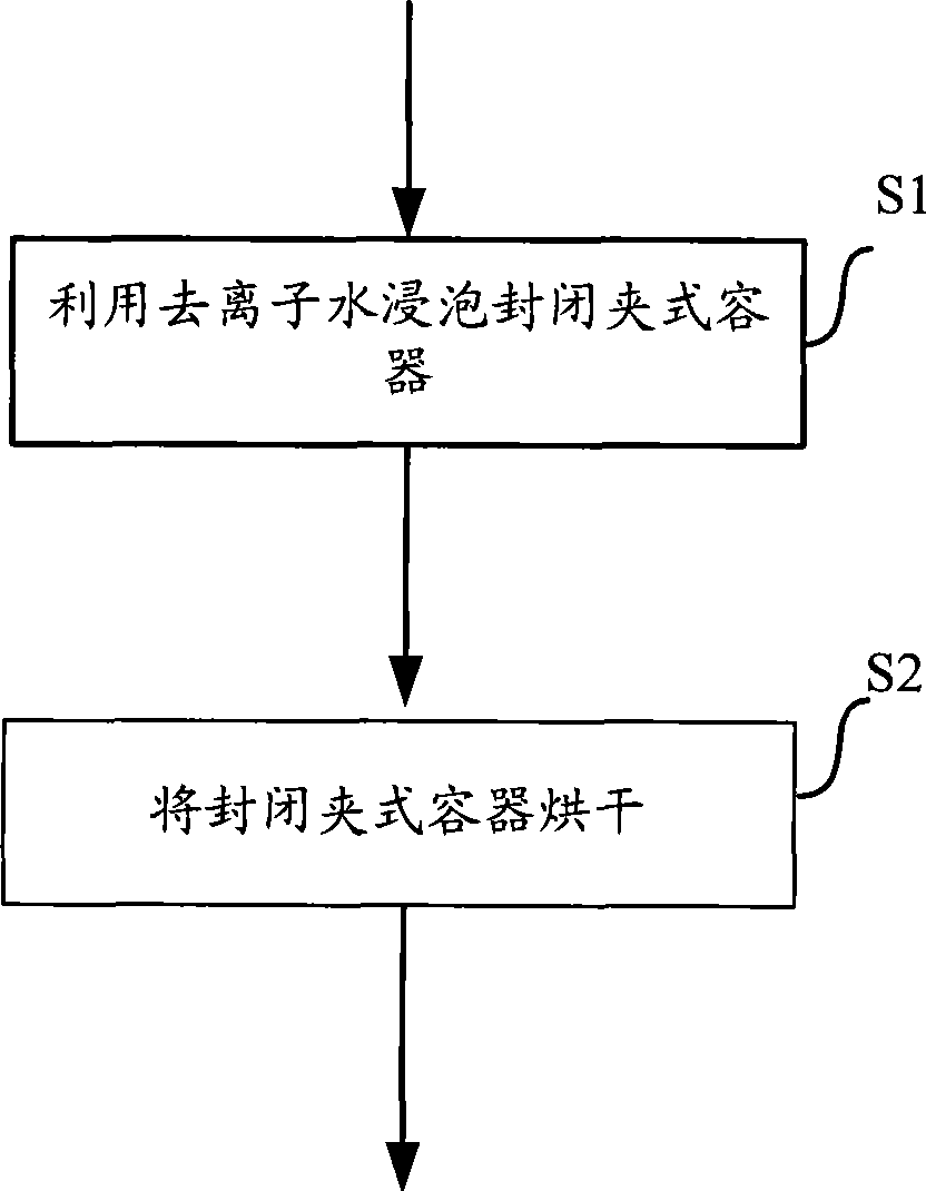
[0023] In this embodiment, what is removed is the fluorine residue on the crystal box. The temperature for soaking the crystal box with deionized water is 70°C, and the time for soaking the crystal box with deionized water is 9 hours.

[0024] In this embodiment, the chemical reaction equation for soaking the crystal box with deionized water is:

[0025]

[0026] Through electron microscope observation, using the method of this embodiment, adsorbed F - The amount of Poly-ether-ether-ketone decreased by 95%. This fully illustrates the superiority of the present invention.

Embodiment 2

[0028] In this embodiment, what is removed is the fluorine residue on the crystal box. The temperature for soaking the crystal box with deionized water is 110° C., and the time for soaking the crystal box with deionized water is 22 hours.

[0029] In this embodiment, the chemical reaction equation for soaking the crystal box with deionized water is:

[0030]

[0031] According to electron microscope observation, the amount of Polyetheretherketone adsorbed F- was reduced by 99% by using the method of this embodiment. This fully illustrates the superiority of the present invention.


PUM


Abstract

The invention discloses a method for removing fluorine residue from the manufacturing of semiconductors and relates to the technical field of semiconductors. The method comprises the following step: a, soaking related parts in deionized water; and b, drying the related parts. Compared with the prior art, the method has the advantages of removing fluorine residue on the related parts from the manufacturing of semiconductors and avoiding crystal defects caused by the fluorine residue.

Description

technical field [0001] The invention relates to the field of integrated circuit technology, in particular to a method for removing fluorine residues in semiconductor manufacturing processes. Background technique [0002] Some fluorine-containing gases are used in semiconductor etching processes. The fluorine-containing gas is ionized into F-, and F- reacts with the material on the wafer to achieve etching. However, a portion of F- will adsorb to the wafer and diffuse through the wafer into various machine parts that the wafer contacts. [0003] The formation of fluorine residues will be specifically described below by taking a crystal box as an example. In the semiconductor manufacturing process, in order to achieve a high degree of local cleaning and reduce the operating cost of the clean room, it is generally necessary to use a crystal box (Pod) to store and transport wafers and other objects to be processed. Typically, wafers are loaded into cassettes after one process...

Claims


Application Information

Patent Timeline
Patent Type & Authority Applications(China)
IPC IPC(8): B08B3/04H01L21/00
Inventor 姜舜杨洪春陈淑美庄祈龙
Owner SEMICON MFG INT (SHANGHAI) CORP
Learn More