Optical contraposition apparatus for joint of circuit apparatus and substrates, and system having the same

A circuit device and alignment device technology, applied in optics, printed circuits, nonlinear optics, etc., can solve problems such as the inability to sense the substrate mark X at the same time, reduce the up and down movement of the camera, and the inability to sense at the same time, so as to improve the operation efficiency. , The effect of improving the good rate and reducing the manufacturing cost

Inactive Publication Date: 2009-08-12
CHROMA ELECTRONICS SHENZHEN
View PDF0 Cites 1 Cited by
  • Summary
  • Abstract
  • Description
  • Claims
  • Application Information

AI Technical Summary

Problems solved by technology

[0005] That is to say, even if the substrate 10 is made of transparent glass, the fixed-focus industrial camera 14 can directly penetrate the sensing substrate 10, but cannot simultaneously sense the mark X on the substrate 10 and the mark X of the circuit device 12; The retracting and resetting process of the substrate 10 is not only time-consuming, but also creates a chance for mechanical errors. When performing alignment operations successively, the fixed-focus industrial camera 14 also needs to be continuously raised and lowered to change the focus position.
[0006] figure 2 It is a schematic diagram of the operation of the zoom-type industrial camera when the known circuit device is bonded to the substrate for alignment. If the sensing lens is replaced with a zoom-type industrial camera 16, the internal movement of the zoom-type industrial camera 16 can reduce the up and down movement of the camera, but still Have the same problem, unable to sense the mark X on the substrate 10 and the circuit device 12 at the same time

Method used


Image

  • Optical contraposition apparatus for joint of circuit apparatus and substrates, and system having the same
  • Optical contraposition apparatus for joint of circuit apparatus and substrates, and system having the same
  • Optical contraposition apparatus for joint of circuit apparatus and substrates, and system having the same

Examples


Embodiment Construction

[0033] The foregoing and other technical contents, features and effects of the present invention will be clearly presented in the following detailed description with accompanying drawings and the preferred embodiments.

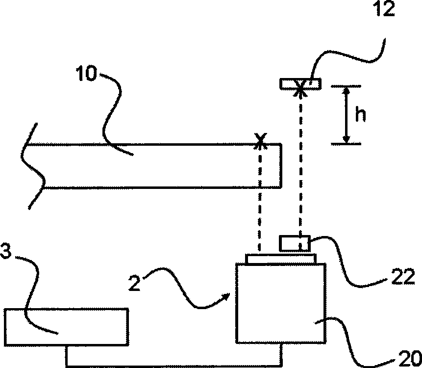
[0034] image 3 It is a schematic diagram of the first preferred embodiment of the application of the present invention. As mentioned above, there is a height difference h between the substrate 10 and the circuit device 12 , and the two need to be precisely aligned and bonded. The optical alignment device 2 of the present invention includes: an optical image capturing unit 20 driven by the control device 3 and synchronously capturing the optical images of the circuit device 12 and the substrate 10 in the height difference direction; . An optical path compensation unit 22 for compensating the optical path difference corresponding to the height difference h between the circuit device 12 and the substrate 10 .

[0035] In order to prevent the circuit device 12 a...


PUM


Abstract

The invention relates to an optical alignment device and a system provided with the same for combining a circuit device with a substrate, which are used for combining the circuit device with the substrate having a height difference with the circuit device through precise alignment. The combining system comprises a bearing device for bearing the substrate, a carrying and moving device for carrying and moving the circuit device, and a set of control device for driving the bearing device and the carrying and moving device to move relatively; and the optical alignment device comprises an optical image acquiring unit which is driven by the control device and is used for acquiring optical images of the circuit device and the substrate synchronously in the direction with the height difference, and an optical path compensating unit which is arranged between the circuit device and the optical image acquiring unit and / or between the substrate and the optical image acquiring unit, and is used for compensating the optical path difference of the height difference of the circuit device and the corresponding substrate. The optical alignment device and the system greatly improve the efficiency of the alignment for the needs of combining the circuit device with the substrate.

Description

technical field [0001] The invention relates to an optical alignment device and a system with the device, in particular to an optical alignment device for bonding a circuit device and a substrate and a system with the device. Background technique [0002] On substrates such as liquid crystal display glass or printed circuit boards, it is often necessary to install integrated circuits or other circuit components. Especially with the complexity of components, the number of pins continues to increase, and the pin density increases accordingly. The efficiency of the bonding process and Accuracy is getting more and more attention, and the industry is devoting great efforts to develop fully automatic machines used in the bonding manufacturing process. Among them, the device responsible for precise positioning of both the circuit device and the substrate to ensure precise alignment during bonding has become an influence on the machine. important factor in performance. [0003] fi...

Claims


Application Information

Patent Timeline
IPC IPC(8): G02F1/13H05K3/00H05K13/04
Inventor 林汉声
Owner CHROMA ELECTRONICS SHENZHEN
Why Eureka
Try Eureka