


Quick Research
Generate reliable direction feasibility study reports for your R&D in just a few steps.

Technical Q&A
Discover and master advanced knowledge NOW. Basics, ideas, possibilities, all at once.

Find Solutions
As an expert in R&D theories, this can generate solutions to your technical problems instantly.

Evaluate Feasibility
Analyze your overall solution with one click, know your potential R&D risks in advance.

Monitor Landscape
Get weekly tech updates, stay abreast of the latest tech innovations and key insights.
Semiconductor device
A semiconductor and regional technology, applied in the direction of semiconductor devices, transistors, electrical components, etc., can solve the problems of difficult low power supply voltage drive, increase of transistor threshold voltage, and decrease of SOI layer body current, and achieve high speed and power supply voltage, low power supply voltage, effect of low threshold voltage
- Summary
- Abstract
- Description
- Claims
- Application Information
AI Technical Summary
Problems solved by technology
Method used
Image

Examples
Embodiment Construction
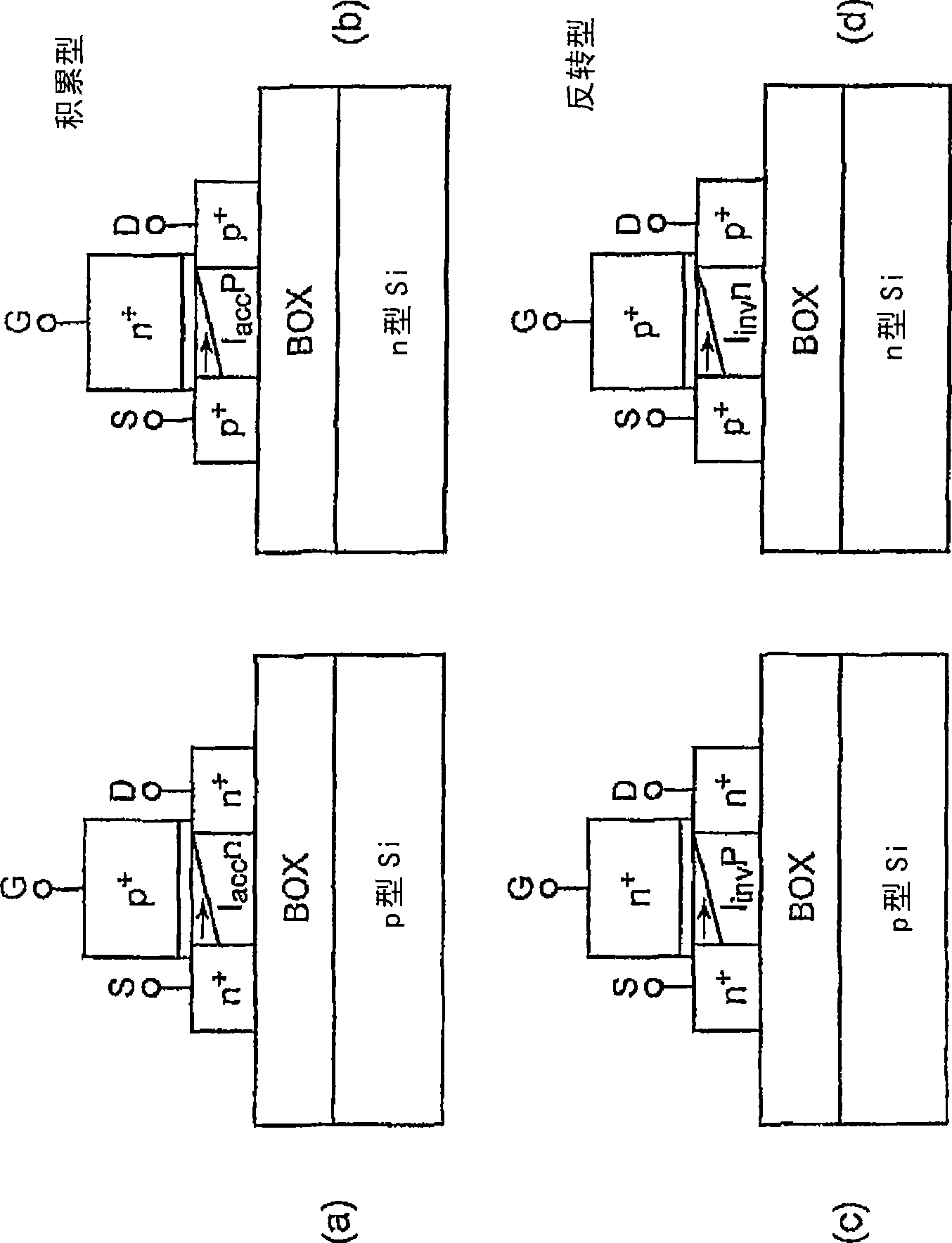
[0034] Next, the semiconductor device of the present invention will be described with reference to the drawings.
[0035] refer to figure 1 , shows an accumulation type (Accumulation) MOS transistor and an inversion type (Inversion) MOS transistor to which the present invention can be applied. here, figure 1 (a) and (b) represent n- and p-channel accumulation type MOS transistors (NMOS transistors and PMOS transistors), respectively, figure 1 (c) and (d) show n-channel and p-channel inversion MOS transistors, respectively.
[0036] exist figure 1In the case of the NMOS transistor shown in (a), an embedded insulating layer (BOX) is formed on the surface region of the p-type silicon substrate, and an n-type SOI (Silicon On Insulator) layer is formed on the embedded insulating layer (BOX) . Furthermore, the n-type SOI layer is formed with source, drain, and channel regions. Wherein, the source and drain regions have a higher impurity concentration than the channel region. ...
PUM
| Property | Measurement | Unit |
|---|---|---|
| Thickness | aaaaa | aaaaa |
Abstract
Description
Claims
Application Information
 - R&D Engineer
- R&D Manager
- IP Professional
- Industry Leading Data Capabilities
- Powerful AI technology
- Patent DNA Extraction
Browse by: Latest US Patents, China's latest patents, Technical Efficacy Thesaurus, Application Domain, Technology Topic, Popular Technical Reports.
© 2024 PatSnap. All rights reserved.Legal|Privacy policy|Modern Slavery Act Transparency Statement|Sitemap|About US| Contact US: help@patsnap.com