Multi-physical field interface multi-scale design method of structure of micro-nano electronic device

An electronic device, multi-physics technology, applied in the field of micro-nano simulation, which can solve the problems of increased computing time and insufficient computing time

Inactive Publication Date: 2009-08-26
JIANGSU UNIV
View PDF0 Cites 8 Cited by
  • Summary
  • Abstract
  • Description
  • Claims
  • Application Information

AI Technical Summary

Problems solved by technology

At present, molecular dynamics is the main means of microscopic modeling. Many microscopic details that cannot be obtained in experiments can be easily observed in molecular dynamics simulations. Molecular dynamics has higher atomic scale than any other method. Therefore, microscopic physical phenomena that cannot be solved by continuum analysis methods can be effectively studied by molecular dynamics. However, the huge time required for molecular dynamics calculations is a very difficult problem to solve. Its calculation time increases sharply with the increase of the number of atoms. In order to reduce the calculation time, the number of atoms used in molecular dynamics simulation is generally relatively small. Even a supercomputer can only simulate 10 9 Atom, that is, a material less than 1 square micron, such a scale range is obviously not enough for the simulation of crack growth, energy impact, etc.

Method used


Image

  • Multi-physical field interface multi-scale design method of structure of micro-nano electronic device
  • Multi-physical field interface multi-scale design method of structure of micro-nano electronic device
  • Multi-physical field interface multi-scale design method of structure of micro-nano electronic device

Examples


Embodiment

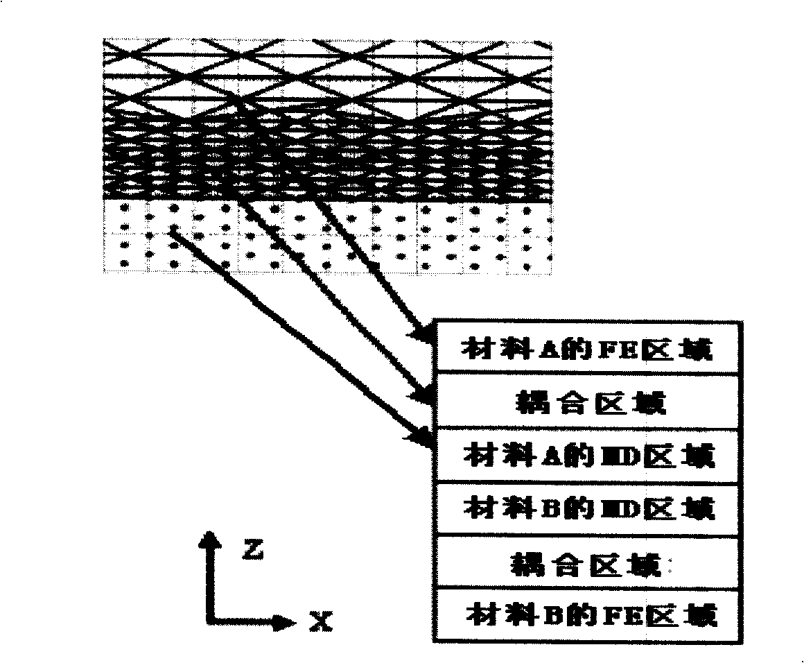
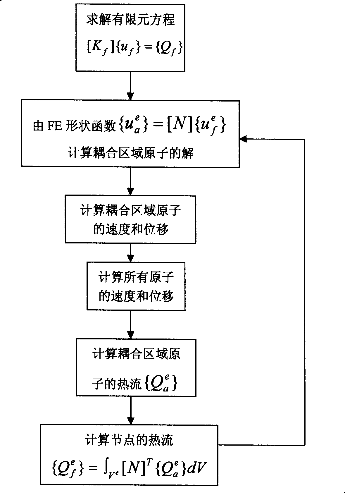
[0022] This embodiment is a simulation of the interface heat transfer characteristics. First, the Green-Lindsay / Lord-Shulman (Green-Lindsay / Lord-Shulman) equation is used to describe the heat transfer coupling mechanism, and then molecular dynamics is used to divide the interface structure into atomic structure integration, and then the finite element is used for Set the thermal load as the boundary condition, and finally program and calculate according to the following steps:

[0023] 1) Solve the finite element equation [K f ]{u f}={Q f}, f stands for unit, K stands for stiffness, u stands for displacement, Q stands for external load, and Q in this embodiment is thermal load.

[0024] 2) Through the finite element shape function { u a e } = [ N ] { u f e } Convert the finite element node temp...


PUM


Abstract

The invention discloses a multi-physical field interface multi-scale design method of structure of a micro-nano electronic device. A coupling system is firstly described, and the molecular dynamics is used for describing the interface tissue evolution and the material defect characteristics; finite elements are used for providing boundary conditions of thermal cycling, bending and stretching actions to a molecular dynamics model; finally, the mathematical simulation of the characteristics of the interface multi-physical field is carried out. The multi-physical field interface multi-scale design method of the structure of the micro-nano electronic device is formed in view of the characteristics of the multi-physical field interface, especially mask interface of the structure of the micro-nano electronic device for researching a framework of a multi-scale model and also in view of influences of the evolution of micro-interface scale material tissues, the production mechanism of thermal defects and material defects consisting holes, cracks, and the like on the physical characteristics of the micro-structure. Both the calculation efficiency and the scientific accuracy are considered. The macroscopical and microcosmic and nanoscopic simulation of whole performance characteristics of the multi-physical field interface of the structure of the micro-nano electronic device is realized. The hard multi-physical field interface multi-scale design problem of the structure of the micro-nano electronic device is solved.

Description

technical field [0001] The invention relates to micro-nano simulation, in particular to a multi-scale coupling design method for studying multi-physics field interfaces of electronic device structures. Background technique [0002] Multilayer structures and multiple interfaces are ubiquitous phenomena in micro-nano electronic devices and device interconnection and packaging. Interface delamination failure has become an important concern in product performance and reliability. Foreign researchers have found through a large number of experiments that the interface is a key part in the manufacture and operation of microsystems, and many damages and defects occur near the interface. However, the research on the interface law of microscopic materials has just started, and the macroscopic theory based on continuum mechanics is no longer applicable. The physical characteristics of the micro-material interface are not only related to the geometry of the microstructure and the distr...

Claims


Application Information

Patent Timeline
Patent Type & Authority Applications(China)
IPC IPC(8): G06F17/50
Inventor 杨平廖宁波
Owner JIANGSU UNIV
Why Eureka
Try Eureka