Radiating modular structure of semiconductor package and manufacturing method thereof

A technology of heat dissipation module and manufacturing method, which is applied in semiconductor/solid-state device manufacturing, semiconductor devices, semiconductor/solid-state device components, etc. It can solve the problems of small area of ​​heat dissipation elements, inability to achieve effective heat dissipation, small size power, etc., to achieve accelerated The effect of large cooling area

Inactive Publication Date: 2009-08-26
SILICONWARE PRECISION IND CO LTD
View PDF4 Cites 5 Cited by
  • Summary
  • Abstract
  • Description
  • Claims
  • Application Information

AI Technical Summary

Problems solved by technology

[0011] The size of the heat dissipation elements combined in the above-mentioned semiconductor packaging structure is limited by the size of the packaging structure itself, and for the semiconductor packaging structure applied to the tape-and-reel package or the flip-chip film technology, all have small size, The characteristics of high power are often limited by the small area of ​​the heat dissipation element of the package structure itself, so that the effect of effective heat dissipation cannot be achieved.

Method used


Image

  • Radiating modular structure of semiconductor package and manufacturing method thereof
  • Radiating modular structure of semiconductor package and manufacturing method thereof
  • Radiating modular structure of semiconductor package and manufacturing method thereof

Examples


Embodiment Construction

[0030] Embodiments of the present invention are described below through specific examples, and those skilled in the art can easily understand other advantages and effects of the present invention from the content disclosed in this specification. The present invention can also be implemented or applied through other different specific embodiments, and various modifications and changes can be made to the details in this specification based on different viewpoints and applications without departing from the spirit of the present invention.

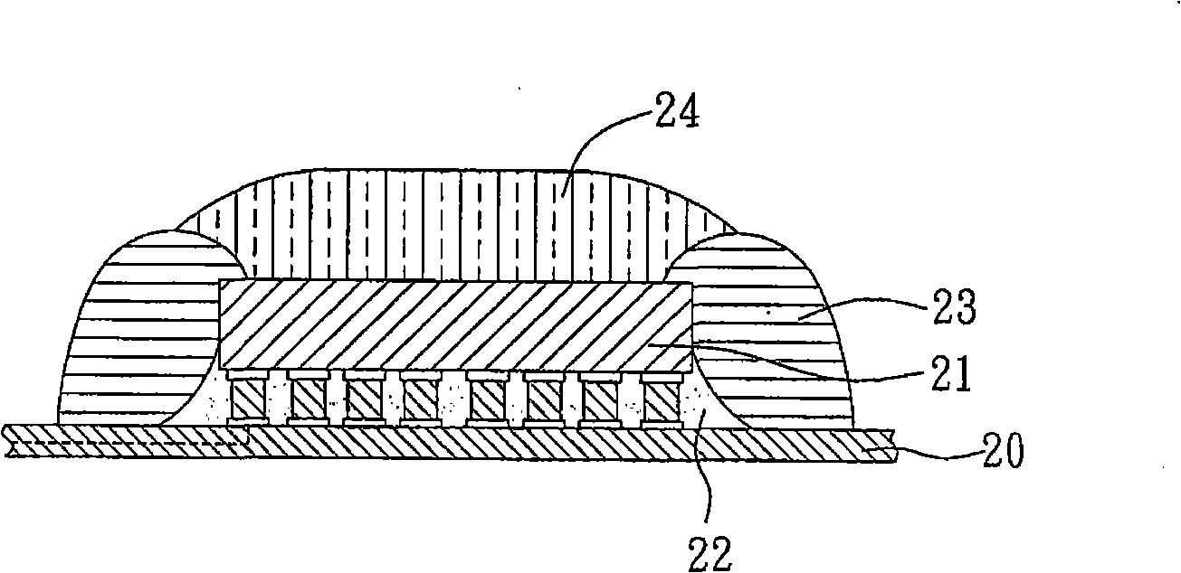
[0031] see Figure 4A to Figure 4C , is a schematic cross-sectional view of the heat dissipation modular structure of the semiconductor package and its manufacturing method of the present invention.

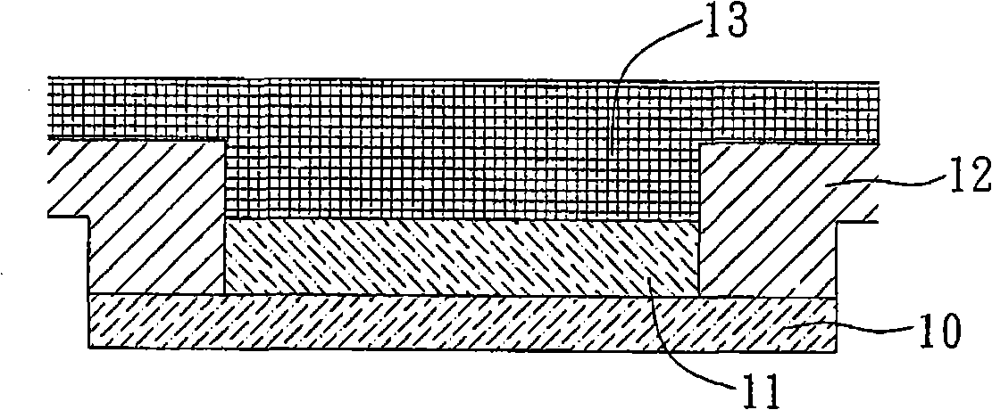
[0032] Such as Figure 4A As shown, at least one semiconductor package 4 is provided, and the semiconductor package 4 includes: a chip carrier 40; at least one semiconductor chip 41 arranged and electrically connected to the chip carrier 40; a ...


PUM


Abstract

The invention relates to a radiating modular structure of a semiconductor package and a manufacturing method. At least one semiconductor semiconductor package comprising a chip carrying piece, a semiconductor chip arranged on the chip carrying piece, and a first radiating piece arranged on the semiconductor chip is provided, so that the semiconductor package is electrically connected to an external electronic device through the chip carrying piece; and then at least one second radiating piece is arranged on the first radiating piece of the semiconductor package, and the size of the second radiating piece is larger than that of the first radiating piece; therefore, the semiconductor package, the first radiating piece, the external electronic device and the second radiating piece are combined in a modular mode to improve the radiating efficiency of the semiconductor package.

Description

technical field [0001] The invention relates to a heat dissipation modular structure and a manufacturing method thereof, in particular to a heat dissipation modular structure of a semiconductor package and a manufacturing method thereof. Background technique [0002] Currently, the prior art of using a flexible carrier board as a packaged chip carrier to electrically connect the chip to the flexible substrate can be roughly divided into tape carrier package (Tape Carrier Package, TCP) and flip chip film (Chip on Film, COF) and other technologies, among which the driver IC packaging process of the display uses the TCP substrate and the COF soft board as the package carrier of the driver IC, which is the largest application of related technologies at present. [0003] However, a highly integrated semiconductor chip will generate a large amount of heat during operation. If the heat generated by the semiconductor chip is not dissipated effectively in time, the performance and li...

Claims


Application Information

Patent Timeline
Patent Type & Authority Applications(China)
IPC IPC(8): H01L21/50H01L23/367
CPCH01L2224/50H01L2224/73204H01L2224/73253
Inventor 程吕义
Owner SILICONWARE PRECISION IND CO LTD
Why Eureka
Try Eureka