
Method for preparing transparent nano imprinting template based on X-ray exposure technology

A nano-imprinting and X-ray technology, applied in optics, opto-mechanical equipment, photosensitive material processing, etc., can solve the problem of engraving high-resolution graphics, etc., and achieve the effect of convenient alignment means

Active Publication Date: 2009-09-02
INST OF MICROELECTRONICS CHINESE ACAD OF SCI
View PDF0 Cites 18 Cited by
  • Summary
  • Abstract
  • Description
  • Claims
  • Application Information

AI Technical Summary

Problems solved by technology

[0004] In view of this, the main purpose of the present invention is to provide a method for making a light-transmitting nanoimprint template based on X-ray exposure technology, so as to solve the problem that high-resolution graphics cannot be obtained by electron beam lithography on a non-conductive substrate. Achieve UV-cured nanoimprinting

Method used


Image

  • Method for preparing transparent nano imprinting template based on X-ray exposure technology
  • Method for preparing transparent nano imprinting template based on X-ray exposure technology
  • Method for preparing transparent nano imprinting template based on X-ray exposure technology

Examples


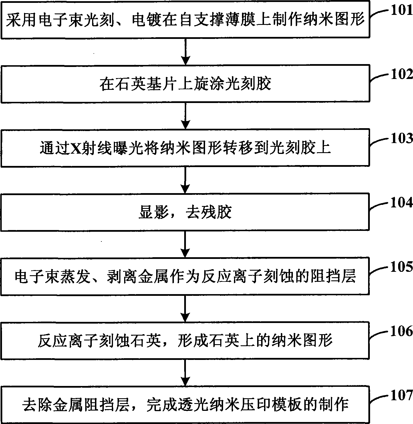
Embodiment Construction

[0027] In order to make the object, technical solution and advantages of the present invention clearer, the present invention will be described in further detail below in conjunction with specific embodiments and with reference to the accompanying drawings.

[0028] The method for making a transparent nano-imprint template provided by the present invention, the transparent nano-imprint template is made of a nano-X-ray exposure template by electron beam lithography, and the nano-pattern is transferred to a non-conductive quartz as a substrate through X-ray exposure. On the bottom of the photoresist, after development, the metal nano-pattern on the quartz substrate is obtained by evaporating metal and stripping process, using the metal as a barrier layer and using reactive ion etching on the quartz to obtain the nano-pattern on the quartz, removing the metal to complete light transmission Fabrication of nanoimprint templates.

[0029] like figure 1 as shown, figure 1 It is a f...


PUM

PropertyMeasurementUnit
thicknessaaaaaaaaaa
thicknessaaaaaaaaaa

Abstract

The invention discloses a method for preparing a transparent nano imprinting template based on an X-ray exposure technology. The transparent nano imprinting template is a nano X-ray exposure template prepared by the electron beam lithography. In the method, with the X-ray exposure, nano patterns are transferred onto a photoresist which adopts non-conductive quartz as a substrate. After development, metal nano patterns on the quartz substrate are obtained with a metal evaporation and stripping technology. As metal is adopted as a barrier layer and reactive ions are used for etching the quartz, the nano patterns on the quartz are obtained and the preparation of the transparent nano imprinting template is completed after the removal of the metal. The invention solves the problem that high resolution patterns cannot be obtained on a non-conductive substrate through the electron beam lithography. Simultaneously, the invention realizes the transparent nano imprinting template and provides a convenient alignment means for nano imprinting, which renders ultraviolet treating nano imprinting possible.

Description

technical field [0001] The invention relates to the field of microfabrication in semiconductor science, in particular to a method for making a light-transmitting nano-imprint template based on X-ray exposure technology. Background technique [0002] Electron beam lithography is a common method for fabricating nanoimprint templates, which is characterized by high resolution and small feature sizes. However, electron beam lithography needs to be carried out on a conductive substrate, and the usual imprint template uses silicon as the substrate material. Since the silicon substrate is opaque, the nanoimprint process using the silicon substrate usually cannot be accurately aligned, and UV-cured nanoimprint cannot be performed. At the same time, using a quartz substrate for electron beam lithography needs to add a conductive layer, the process is complicated, and the resolution is not high. Contents of the invention [0003] (1) Technical problems to be solved [0004] In vi...

Claims


Application Information

Patent Timeline
Patent Type & Authority Applications(China)
IPC IPC(8): G03F7/00G03F7/16G03F7/42
Inventor 刘兴华徐德钰朱效立谢常青刘明
Owner INST OF MICROELECTRONICS CHINESE ACAD OF SCI
Learn More