Liquid crystal display divice

A technology of liquid crystal display device and display area, applied in transistors, static indicators, optics, etc., can solve problems such as complex manufacturing process

Active Publication Date: 2009-09-09
JAPAN DISPLAY INC +1
View PDF1 Cites 4 Cited by
  • Summary
  • Abstract
  • Description
  • Claims
  • Application Information

AI Technical Summary

Problems solved by technology

However, forming TFTs with different structures on one substrate complicates the manufacturing process

Method used


Image

  • Liquid crystal display divice
  • Liquid crystal display divice
  • Liquid crystal display divice

Examples


Embodiment 1

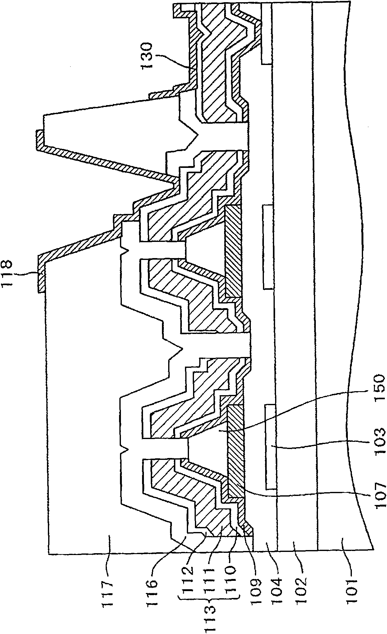
[0051] In the liquid crystal display device of this embodiment, pixels are formed on a region surrounded by image signal lines extending vertically and arranged horizontally and scanning signal lines extending horizontally and arranged vertically, and a pixel electrode and a pixel electrode are arranged in each pixel. TFT for switching. Pixels including pixel electrodes and TFTs are arranged in a matrix on the display area. A drive circuit for controlling supply of an image signal to each pixel is provided on the periphery of the display area. In this embodiment, bottom-gate poly-Si TFTs are used for both the TFTs used in the pixel portion and the TFTs used in the driver circuit. Here, poly-Si TFT means using poly-Si as a semiconductor.

[0052] figure 1 is a schematic cross-sectional view showing the structure of the present invention. exist figure 1 In the figure, the TFT on the left is a TFT used in the driver circuit section. The TFT on the right is a TFT used in t...

Embodiment 2

[0072] In this embodiment, the TFT used in the pixel portion is a bottom-gate a-Si TFT, and the TFT used in the driver circuit portion is a bottom-gate poly-Si TFT. Here, a-Si TFT means using a-Si in the semiconductor layer, and poly-Si TFT means using poly-Si in the semiconductor layer. This is because poly-Si TFTs that operate faster because of their high mobility are advantageous in the driver circuit section, and a-Si TFTs that are easy to reduce leakage current are advantageous in the pixel section.

[0073] Figure 10 is a schematic cross-sectional view showing the structure of the second embodiment of the present invention. exist Figure 10 In the figure, the TFT on the left is a TFT used in the driver circuit section, and the TFT is formed of poly-Si. TFTs for driving circuits require high-speed operation, so poly-Si-based TFTs are used. The TFT on the right is a TFT used in the pixel portion, and the TFT is made of a-Si. This is because a small leakage current is...


PUM

PropertyMeasurementUnit
thicknessaaaaaaaaaa
thicknessaaaaaaaaaa

Abstract

The invention provides a liquid crystal display device. In bottom-gate-type thin film transistors used in a liquid crystal display device, a channel stopper layer is formed on a poly-Si layer thus stabilizing a characteristic of the thin film transistor. The channel stopper layer is formed into a desired shape by wet etching, and the poly-Si layer is formed into a desired shape by dry etching. By applying side etching to the channel stopper layer, a peripheral portion of the poly-Si layer is exposed from the channel stopper layer, and this region is brought into contact with an n+Si layer. Due to such constitution, ON resistance of the thin film transistor can be decreased thus increasing an ON current which flows in the thin film transistor.

Description

technical field [0001] The present invention relates to a display device, and more particularly, to a liquid crystal display device having pixels using TFTs for switching in a display region and a driver circuit composed of TFTs using poly-Si formed around the display region. Background technique [0002] In a liquid crystal display device, a TFT substrate is opposed to a color filter substrate, and a liquid crystal is sandwiched between the TFT substrate and the color filter substrate. Pixel electrodes and thin-film transistors (TFTs) are formed in a matrix on the TFT substrate. etc., color filters and the like are formed on the color filter substrate at positions corresponding to the pixel electrodes. [0003] On the TFT substrate there are data lines extending vertically and arranged horizontally and scanning lines extending horizontally and arranged vertically, and pixels are formed on the area surrounded by the data lines and the scanning lines. A pixel is mainly compo...

Claims


Application Information

Patent Timeline
Patent Type & Authority Applications(China)
IPC IPC(8): G02F1/1362G09G3/36H01L27/12H01L21/84G02F1/1345G02F1/1368H01L21/336H01L29/786
CPCG02F2202/103H01L29/78609G02F1/1368H01L27/1214G02F2202/104H01L27/1288H01L29/66765G02F1/1303
Inventor 海东拓生园田大介新田秀和
Owner JAPAN DISPLAY INC
Why Eureka
Try Eureka