Appearance inspection device and inspection method for component installation state

A technology for inspection devices and patterns, applied in measurement devices, electrical components, electrical components, etc., can solve the problems of inability to determine the color of solder, large color changes, and rising equipment costs, and achieve shortened program generation time, fewer production steps, and errors. Judgment less effect

Inactive Publication Date: 2009-09-16
北原明 +1
View PDF3 Cites 1 Cited by
  • Summary
  • Abstract
  • Description
  • Claims
  • Application Information

AI Technical Summary

Problems solved by technology

In order to prevent the solder 40 and foreign matter from falling, a dedicated jig is required separately, which increases the cost of equipment
[0013] Furthermore, in image processing, in JP-A-6-18237, it is too time-consuming to set inspection ranges separately.
In addition, in Japanese Patent Laid-Open No. 2005-156381, good or bad is judged by the area of ​​the solder, but the surface of the solder has unevenness that changes every printing, and the color changes greatly, and dark parts may also occur.
[0014] In particular, it is difficult to distinguish whether the dark part is solder or the adjacent protective layer, and it will change as above, so the color of the solder cannot be determined
Therefore, it is difficult to accurately accumulate the solder area, which may lead to misjudgment due to insufficient solder and misjudgment of the bridge

Method used


Image

  • Appearance inspection device and inspection method for component installation state
  • Appearance inspection device and inspection method for component installation state
  • Appearance inspection device and inspection method for component installation state

Examples


no. 1 example

[0056] Hereinafter, an embodiment of the present invention will be described in detail using the drawings. First, the configuration of the inspection device will be described in detail.

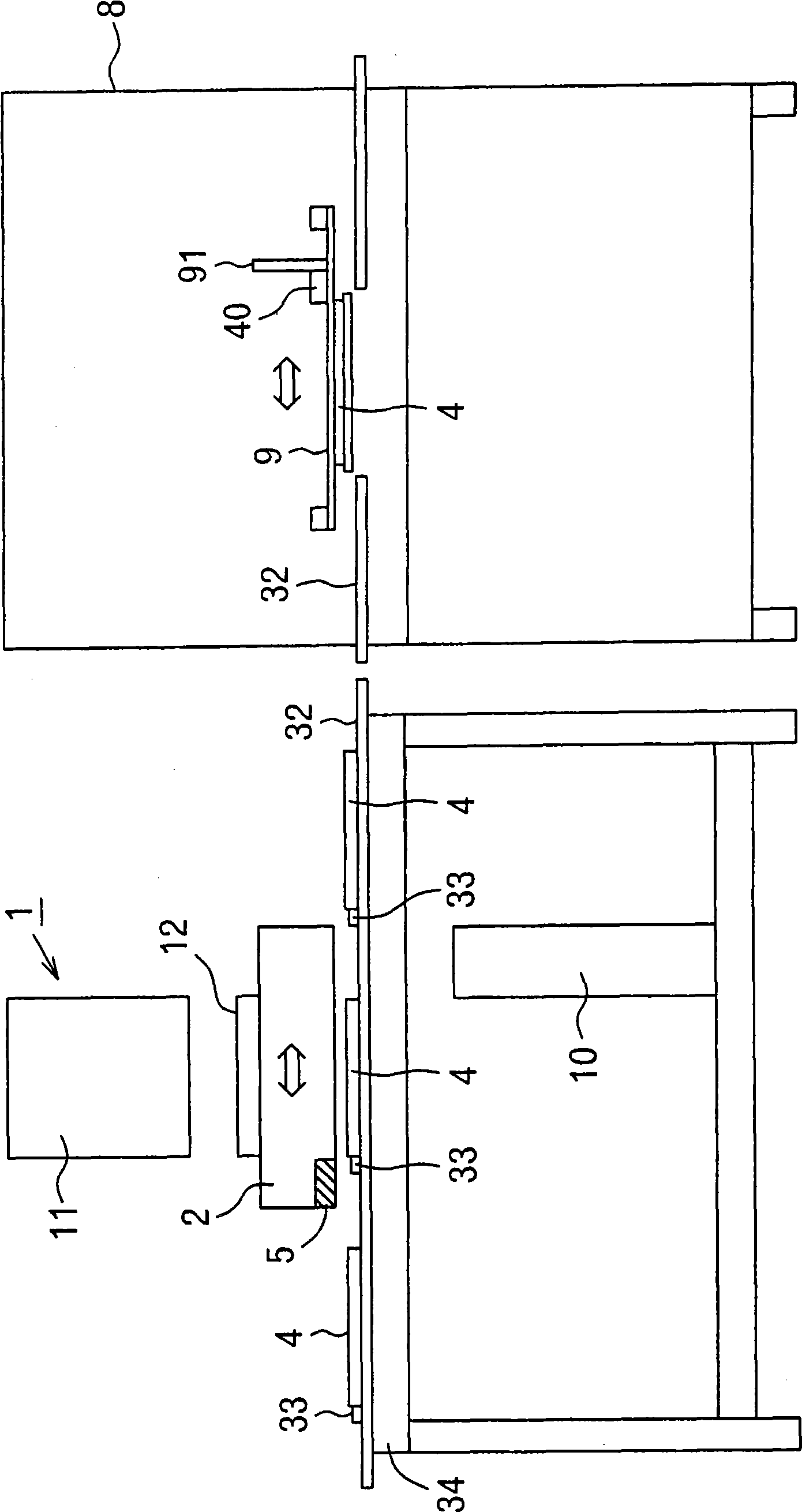
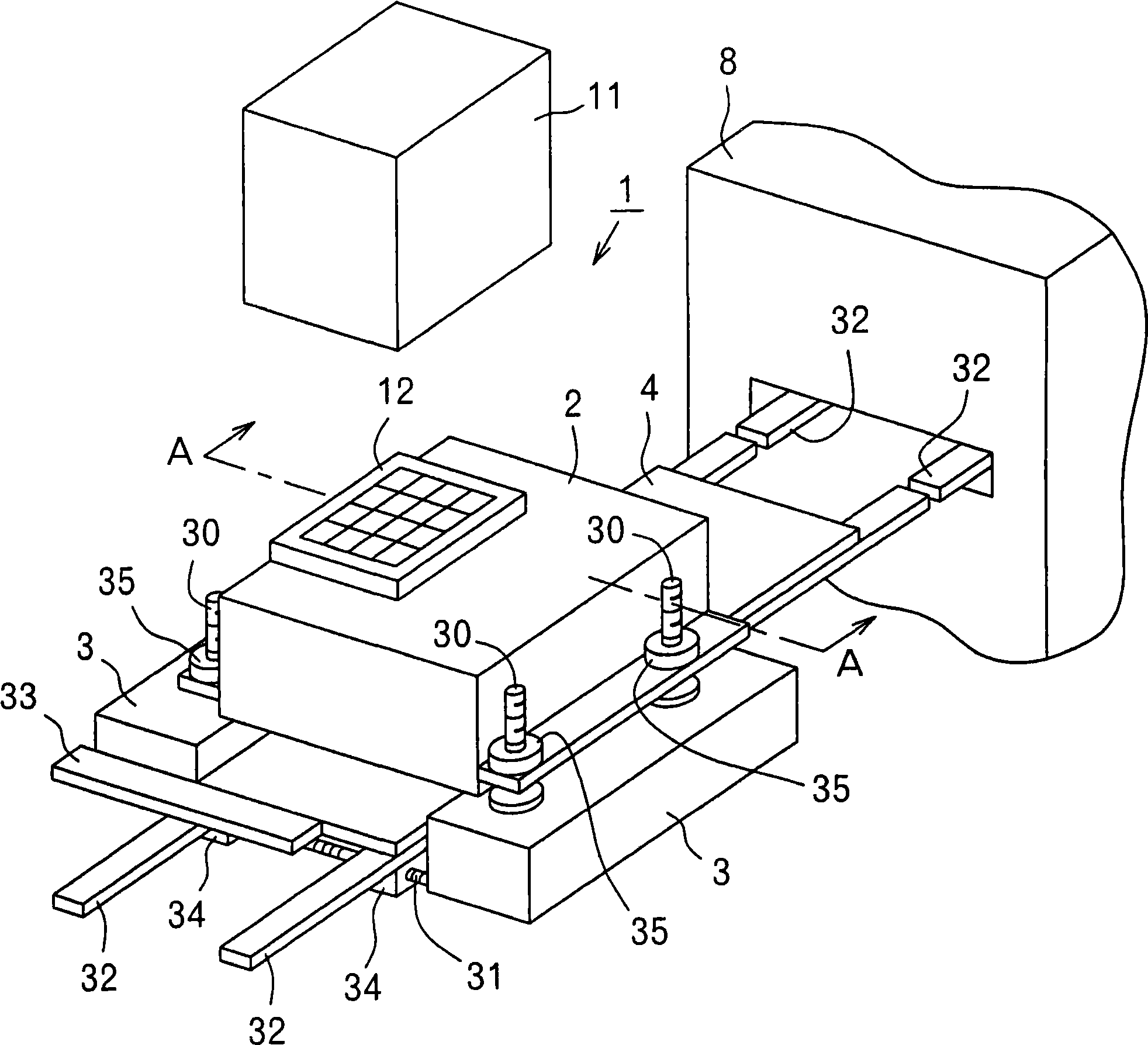
[0057] figure 1 It is a front view showing the outline of the inspection device 1 . figure 2 is a perspective view of the inspection device 1 .

[0058] The inspection device 1 is provided on a conveyor belt 32 extending left and right and driven intermittently, and a plurality of printed circuit boards 4 , 4 to be soldered are placed on the conveyor belt 32 to be separated from each other. A printing machine 8 is provided on the upstream side of the conveyor belt 32 from the inspection device 1 . An electronic component mounter for mounting electrons on the printed circuit board 4 and a reflow furnace (not shown) for thermally hardening solder are provided on the downstream side of the conveyor belt 32 from the inspection device 1 . The conveyor belt 32 of the printing press 8 and the ...

no. 2 example

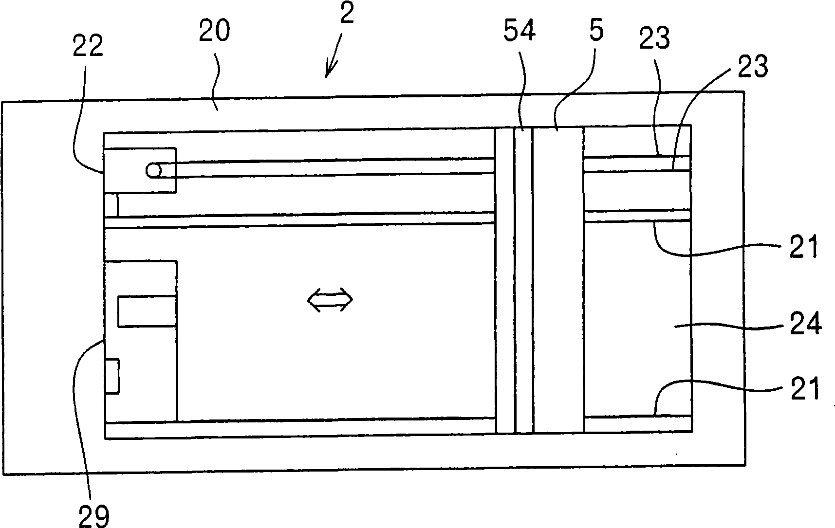
[0083] Figure 11 It is a plan view showing an image scanner 2 of another embodiment. A general commercially available scanner reads A4 size (length 21 cm x width 30 cm) at the maximum, and if the size of the printed circuit board 4 is increased in resolution by A4 size, the scanning time will become longer. In this example, three reading modules, namely, the first reading module 5 , the second reading module 50 and the third reading module 51 are provided in the image scanner 2 . For ease of illustration, the guide shafts 21, 21 are not shown. The 1 / 3 area from the upstream side of the printed substrate 4, that is, the right side, is scanned by the first reading module 5, and the 1 / 3 area from the downstream side of the printed substrate 4, that is, the left side, is scanned by the second reading module 50. image. which is, Figure 12 Among them, the image of area X is scanned by the first reading module 5 , and the image of area Y is scanned by the second reading module ...

no. 3 example

[0088] Figure 14 It is a plan view showing an image scanner 2 of another embodiment. In this example, with multiple Figure 14 In the middle are ten vertical reading modules 52, 52, which do not move. Instead, the printed substrate 4 on the conveyor belt 32 moves. This requires inspection at a high resolution of about 5 to 10 micrometers in the inspection of damage, stains, foreign matter, and patterns on the printed circuit board 4 , which is considerably time-consuming. Therefore, by providing a plurality of vertical reading modules 52, 52 with a smaller planar area than the horizontal type, the inspection surface is divided, the moving distance of the printed circuit board 4 is shortened, and the scanning time is reduced. Furthermore, the number of vertical reading modules 52, 52 is not limited to Figure 14 the number shown.


PUM

PropertyMeasurementUnit
lengthaaaaaaaaaa
lengthaaaaaaaaaa

Abstract

Provided is an appearance inspection device and inspection method for a component installation state, wherein the inspection device (1) is provided with an image scanner (2), having at least a reading module (5) moving along a guide shaft (21) and making an image reading part (54) towards a lower side to scan an image, and a horizontal supporting member for supporting the reading module (5) horizontally; a conveyor belt (32), conveyed to the lower side of the image reading part (54) of the image scanner (2) as a printing substrate (4) of an inspection object; and a mechanism for processing the image scanned by the reading module (5) and displaying on a monitor (11).

Description

technical field [0001] The present invention relates to an appearance inspection device for the mounting state of electronic components, and mainly relates to a device and an inspection method for inspecting the soldering state of a printed circuit board on which solder paste is printed. Background technique [0002] Conventionally, as a method of printing solder paste 40 on the printed circuit board 4, Figure 15 process shown. The solder paste 40 refers to solder containing metal in a paste form. [0003] The printed circuit board 4 is provided on the lower side of the metal mask 9 in which a plurality of holes 90 , 90 are opened. A mass of paste solder paste 40 is placed on one end portion of the metal mask 9 , and the solder 40 is filled into the hole 90 by a squeegee 91 serving as a press-fitting plate. The solder 40 inside the hole 90 is printed onto the printed substrate 4 . [0004] As is well known, a pattern 41 made of copper is formed on the printed circuit boa...

Claims


Application Information

Patent Timeline
Patent Type & Authority Applications(China)
IPC IPC(8): G01N21/956
CPCG01N21/956H01L21/67288H05K13/08
Inventor 北原明北原秀晋
Owner 北原明
Why Eureka
Try Eureka