Electrifying circuit on mobile terminal camera
A mobile terminal and camera technology, applied in the field of cameras, can solve problems such as prolonging the time to market of products and increasing R&D investment, and achieve the effects of shortening project cycle, reducing R&D costs and enhancing compatibility
- Summary
- Abstract
- Description
- Claims
- Application Information
AI Technical Summary
Problems solved by technology
Method used
Image

Examples
Embodiment Construction
[0021] The specific implementation manner of the present invention will be further described in detail below in conjunction with the accompanying drawings and examples, but the protection scope of the present invention should not be limited thereby.
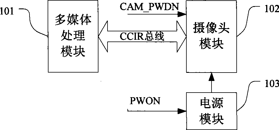
[0022] figure 1 It is a schematic diagram of the camera module system of the mobile terminal. The camera system of the mobile terminal mainly includes a multimedia processing module 101 , a camera module 102 and a power module 103 . Wherein the camera is connected to the multimedia processing module through a CCIR (Consultative Committee Intemathnal Radio) bus. The multimedia processing module 101 may be a baseband chip or an external multimedia processor. PWON and CAM_PWDN are control signals from the baseband chip or an external multimedia processor. PWON is the camera power enable signal, and CAM_PWDN is the power-down control signal of the camera module. PWON and CAM_PWDN are control signals from the baseband chip or an e...
PUM
 Abstract
Description
Claims
Application Information
PatSnap Eureka turns technology decisions into work you can execute. Powered by our Innovation Knowledge Graph, it runs expert workflows across engineering, life sciences, materials and intellectual property. Get your review-ready output in minutes.


