High-side NLDMOS structure

A high-side, N-type technology, applied in the field of high-side NLDMOS structure, can solve the problem of low drain-source breakdown voltage and achieve the effect of improving off-state breakdown voltage

Inactive Publication Date: 2009-09-23
ZHEJIANG UNIV
View PDF0 Cites 18 Cited by
  • Summary
  • Abstract
  • Description
  • Claims
  • Application Information

AI Technical Summary

Problems solved by technology

[0008] The technical problem to be solved by the present invention is to provide a high-side NLDMOS structure to overcome the disadvantages of the prior art that the potential line is concentrated between the source terminal and the NBL when the device is off, resulting in a low drain-source breakdown voltage

Method used


Image

  • High-side NLDMOS structure
  • High-side NLDMOS structure
  • High-side NLDMOS structure

Examples


Embodiment Construction

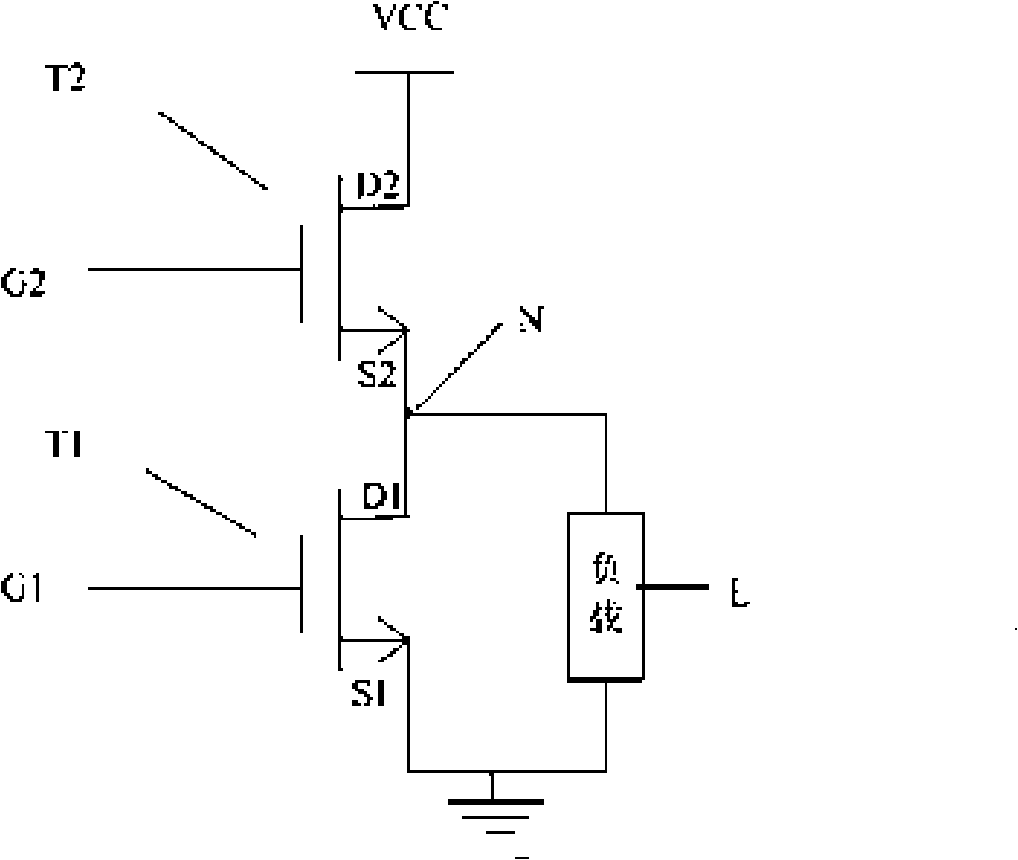
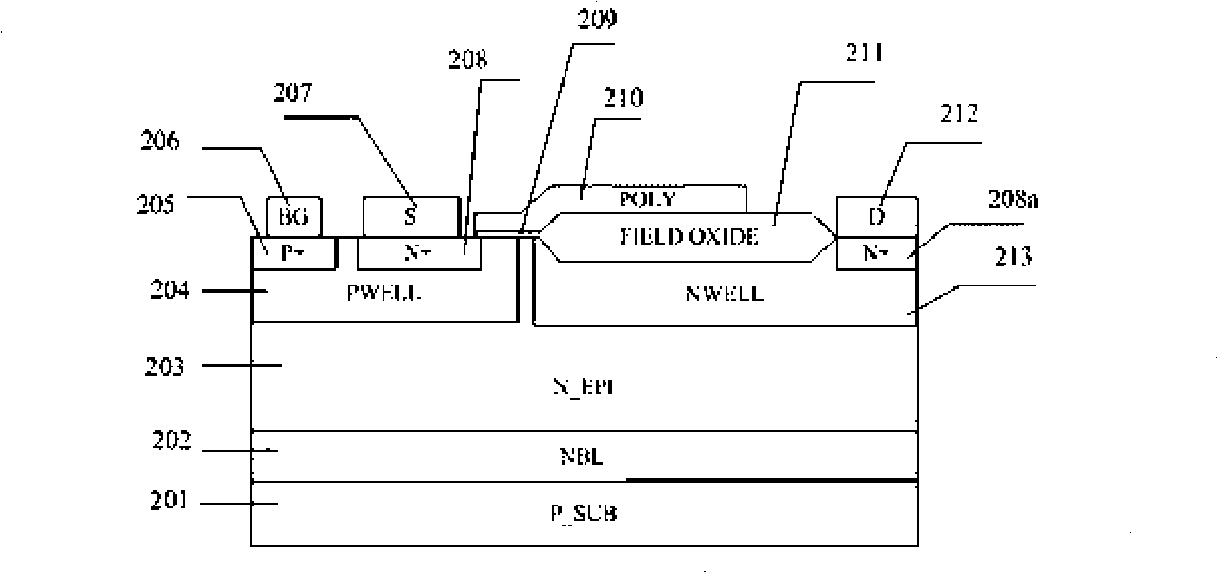
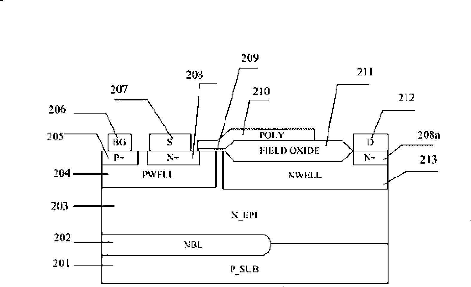
[0017] Embodiments of the present invention: the present invention will be further described in conjunction with the drawings and embodiments of the description. image 3 is a schematic structural diagram of the high-side NLDMOS of the present invention. A portion of the N-type buried layer 202 is located above the P substrate 201 . An N-type epitaxy 203 is above part of the N-type buried layer 202 and part of the P-substrate 201 . The top of the N-type epitaxy 203 is a well region. The P well 204 forms the channel of the LDMOS, and the N well 213 forms the drain drift region of the device. The P+ injection region 205 in the P well 204 is connected to the back gate electrode 206 of the device, the N+ injection region 208 is connected to the source electrode 207 ; the N+ injection region 208a in the N well 213 is connected to the drain electrode 212 . The gate electrode 210 is made of polysilicon, covers the gate oxide 209 , and partly extends to the field oxide 211 to funct...


PUM


Abstract

The invention discloses a high-side NLDMOS structure. On the basis of the original high-side NLDMOS, an N-type buried layer (202) of a whole section which is originally arranged between a P-type substrate (201) and an N-type extension (203) is changed into the N-type buried layer (202) of a partial section. Generally speaking, the length of the N-type buried layer (202) ranges from one third to two thirds of the whole length of the P-type substrate (201). Generally, the length of the N-type buried layer (202) is produced to be about half of the whole length of the P-type substrate (201). The high-side NLDMOS structure not only prevents the breakdown between a source and the substrate when an element is in on-state, but also causes electric potential wires to be evenly distributed at a source terminal and a drain terminal when the element is in off-state; and the high-side NLDMOS structure also improves the breakdown voltage of the off-state of the element, without increasing the extension layer thickness or the area of the element or affecting the performance of the element. The high-side NLDMOS structure can be applied to circuits of chips for motor driving, power supply management, flat-panel display driving, and the like.

Description

technical field [0001] The invention relates to a high-side NLDMOS structure, which belongs to the field of high-voltage power devices and can be applied to circuits of chips such as motor drive, power management, and flat panel display drive. Background technique [0002] LDMOS (Lateral Diffused Medal-Oxide-Semiconductor) is a lateral double-diffused MOS structure. It utilizes the difference between the two diffusions of boron and phosphorus to form a channel, and can precisely control the channel length by using the redistribution temperature and time, so the channel length can not be limited by the minimum size of lithography. LDMOS has a long low-concentration drift region between the channel and the drain, which plays a role in increasing the device's off-state breakdown voltage. [0003] On-state on-resistance (Rdson) and off-state breakdown voltage (BVdss) are the two most important parameters of LDMOS. The smaller the Rdson, the stronger the driving ability of LDMO...

Claims


Application Information

Patent Timeline
IPC IPC(8): H01L29/78H01L29/06H01L23/52
CPCH01L29/0878H01L29/1083H01L29/42368H01L29/7816
Inventor 韩成功韩雁张斌张世峰胡佳贤
Owner ZHEJIANG UNIV
Why Eureka
Try Eureka