
Camera chip size module with novel structure and method for producing same

A technology with a chip size and a new structure, applied in the field of electron optics, can solve the problems of printed circuit board size inconsistency, waste of data and inventory, bulky volume, etc., and achieve the effect of convenient and flexible assembly operation, precise focal length, and small size

Inactive Publication Date: 2009-09-23
王美云
View PDF0 Cites 0 Cited by
  • Summary
  • Abstract
  • Description
  • Claims
  • Application Information

AI Technical Summary

Problems solved by technology

[0002] With the rapid growth of video transmission technology, the requirements for image input terminals have also expanded. At present, camera modules are used to achieve the purpose, and the existing camera and circuit board are separate components. When assembling, the camera needs to be set on the circuit board. The surface of the board is bulky, inconvenient to operate, and may easily cause dust pollution. At the same time, the size of the PCB printed circuit board cannot be unified, resulting in data waste and inventory accumulation.

Method used


Image

  • Camera chip size module with novel structure and method for producing same

Examples


Embodiment Construction

[0017] Below in conjunction with accompanying drawing, the present invention is described in further detail with preferred embodiment:

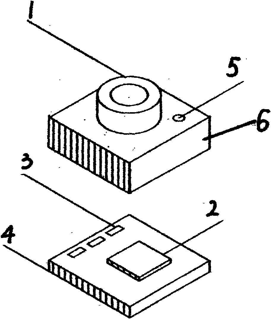
[0018] The present invention consists of a lens (1), a sensor (2), components (3), a circuit board (4) and an exhaust hole (5). The circuit board (4) and components (3) are ultra-miniature designs, and A sensor (2) is provided in the middle of the surface of the board (4), components (3) are provided at the edge, an air vent (5) is provided on the lens base (6), the size of the circuit board (4) is equal to the size of the chip package, and the circuit board (4) is The board (4), the sensor (2) and the components (3) are ultra-precisely assembled inside the lens base (6).

[0019] Production method of the present invention is:

[0020] 1. The use of high-temperature materials (Reflowable) solves the problem of fine dust generated by the assembly process. Its high-temperature material technologies include:

[0021] a. Glass molded lens repla...


PUM


Abstract

The invention relates to a camera chip size module with a novel structure and a method for producing the same. At present, a video transmission technique adopts a camera module technique, has separated components of a camera and a circuit board which have bulky volumes and inconvenient operation, and is likely to cause problems of easy generation of particulate pollutions, impossibility of unifying the sizes of printed circuit boards, data wastes, inventory accumulation and the like. The camera chip size module consists of a lens, a sensor, an element, a circuit board and vent holes, wherein the middle part on the surface of the circuit board is provided with the sensor and the edge part thereof is provided with the element, a pedestal of the lens is provided with the vent holes, the circuit board size is equal to the chip packaging size, and the circuit board, the sensor and the element are assembled in the pedestal of the lens ultra-precisely. By making use of a high temperature material, the particulate problem is solved; and by making use of a chip level packaging technique to minimize and standardize the module, the inventory problem is solved. The camera chip size module has the advantages of small volume, simple structure, no particulates, precise focal distance, vent hole design for the convenience of high temperature machining, convenient and flexible assembling operations, extensive range of application, and advantageous popularization.

Description

technical field [0001] The invention relates to the field of electron optics, in particular to a camera chip size module with a novel structure and a production method thereof. Background technique [0002] With the rapid growth of video transmission technology, the requirements for image input terminals have also expanded. At present, camera modules are used to achieve the purpose, and the existing camera and circuit board are separate components. When assembling, the camera needs to be set on the circuit board. The surface of the board is bulky, inconvenient to operate, and easily causes dust pollution. At the same time, the size of the PCB printed circuit board cannot be unified, resulting in waste of materials and inventory accumulation. Contents of the invention [0003] The object of the present invention is to provide a camera chip size module and its production method with a new structure that utilizes chip-level packaging technology, minimizes and standardizes the...

Claims


Application Information

Patent Timeline
IPC IPC(8): H04N5/225H01L25/00H01L25/16H01L21/50
Inventor 王美云
Owner 王美云
Learn More